© 2003 Fairchild Semiconductor Corporation
DS005352
www.fairchildsemi.com
February 1984
Revised October 2003
MM74HC4046 CM
OS Phase Lock
Loo
p
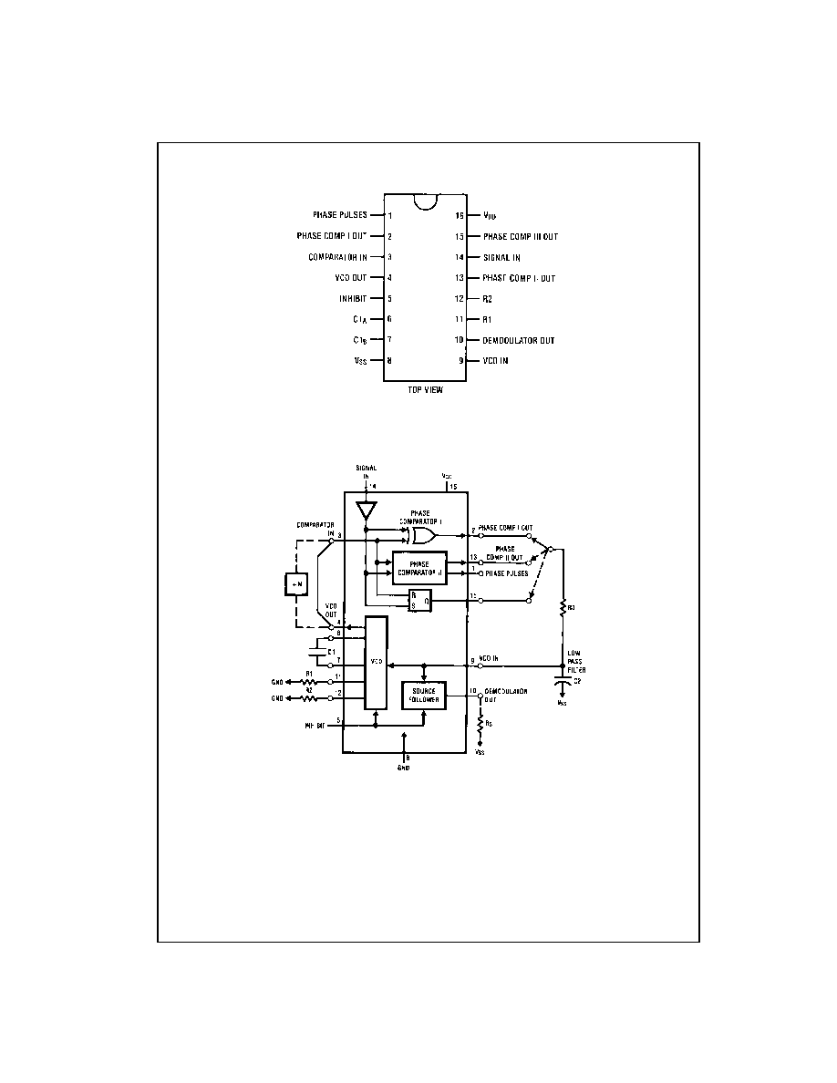
MM74HC4046
CMOS Phase Lock Loop
General Description
The MM74HC4046 is a low power phase lock loop utilizing
advanced silicon-gate CMOS technology to obtain high fre-
quency operation both in the phase comparator and VCO
sections. This device contains a low power linear voltage
controlled oscillator (VCO), a source follower, and three
phase comparators. The three phase comparators have a
common signal input and a common comparator input. The
signal input has a self biasing amplifier allowing signals to
be either capacitively coupled to the phase comparators
with a small signal or directly coupled with standard input
logic levels. This device is similar to the CD4046 except
that the Zener diode of the metal gate CMOS device has
been replaced with a third phase comparator.
Phase Comparator I is an exclusive OR (XOR) gate. It pro-
vides a digital error signal that maintains a 90 phase shift
between the VCO's center frequency and the input signal
(50% duty cycle input waveforms). This phase detector is
more susceptible to locking onto harmonics of the input fre-
quency than phase comparator I, but provides better noise
rejection.
Phase comparator III is an SR flip-flop gate. It can be used
to provide the phase comparator functions and is similar to
the first comparator in performance.
Phase comparator II is an edge sensitive digital sequential
network. Two signal outputs are provided, a comparator
output and a phase pulse output. The comparator output is
a 3-STATE output that provides a signal that locks the VCO
output signal to the input signal with 0 phase shift between
them. This comparator is more susceptible to noise throw-
ing the loop out of lock, but is less likely to lock onto har-
monics than the other two comparators.
In a typical application any one of the three comparators
feed an external filter network which in turn feeds the VCO
input. This input is a very high impedance CMOS input
which also drives the source follower. The VCO's operating
frequency is set by three external components connected
to the C1A, C1B, R1 and R2 pins. An inhibit pin is provided
to disable the VCO and the source follower, providing a
method of putting the IC in a low power state.
The source follower is a MOS transistor whose gate is con-
nected to the VCO input and whose drain connects the
Demodulator output. This output normally is used by tying
a resistor from pin 10 to ground, and provides a means of
looking at the VCO input without loading down modifying
the characteristics of the PLL filter.
Features
s
Low dynamic power consumption:
(V
CC
=
4.5V)
s
Maximum VCO operating frequency:
12 MHz (V
CC
=
4.5V)
s
Fast comparator response time (V
CC
=
4.5V)
Comparator I:
25 ns
Comparator II:
30 ns
Comparator III:
25 ns
s
VCO has high linearity and high temperature stability
Ordering Code:
Devices also available in Tape and Reel. Specify by appending the suffix letter "X" to the ordering code.
Order Number
Package Number
Package Description
MM74HC4046M
M16A
16-Lead Small Outline Integrated Circuit (SOIC), JEDEC MS-012, 0.150" Narrow
MM74HC4046SJ
M16D
16-Lead Small Outline Package (SOP), EIAJ TYPE II, 5.3mm Wide
MM74HC4046MTC
MTC16
16-Lead Thin Shrink Small Outline Package (TSSOP), JEDEC MO-153, 4.4mm Wide
MM74HC4046N
N16E
16-Lead Plastic Dual-In-Line Package (PDIP), JEDEC MS-001, 0.300" Wide
3
www.fairchildsemi.com
MM74HC4046
Absolute Maximum Ratings
(Note 1)
(Note 2)
Recommended Operating
Conditions
Note 1: Maximum Ratings are those values beyond which damage to the
device may occur.
Note 2: Unless otherwise specified all voltages are referenced to ground.
Note 3: Power Dissipation temperature derating -- plastic "N" package:
-
12 mW/
∞
C from 65
∞
C to 85
∞
C.
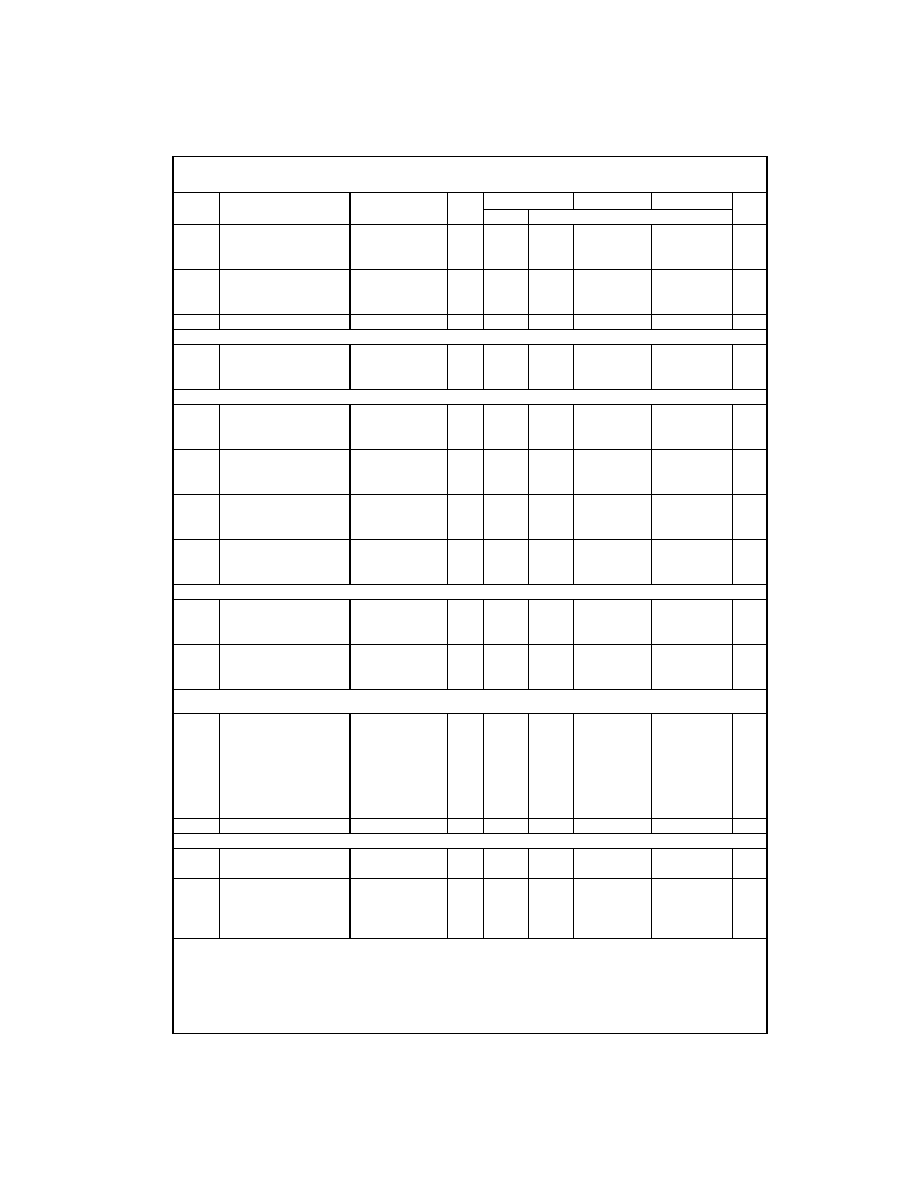
DC Electrical Characteristics
(Note 4)
Note 4: For a power supply of 5V
±
10% the worst case output voltages (V
OH
, and V
OL
) occur for HC at 4.5V. Thus the 4.5V values should be used when
designing with this supply. Worst case V
IH
and V
IL
occur at V
CC
=
5.5V and 4.5V respectively. (The V
IH
value at 5.5V is 3.85V.) The worst case leakage cur-
rent (I
IN
, I
CC
, and I
OZ
) occur for CMOS at the higher voltage and so the 6.0V values should be used.
Supply Voltage (V
CC
)
-
0.5 to
+
7.0V
DC Input Voltage (V
IN
)
-
1.5 to V
CC
+
1.5V
DC Output Voltage (V
OUT
)
-
0.5 to V
CC
+
0.5V
Clamp Diode Current (I
IK
, I
OK
)
±
20 mA
DC Output Current per pin (I
OUT
)
±
25 mA
DC V
CC
or GND Current, per pin (I
CC
)
±
50 mA
Storage Temperature Range (T
STG
)
-
65
∞
C
+
150
∞
C
Power Dissipation (P
D
)
(Note 3)
600 mW
S.O. Package only
500 mW
Lead Temperature (T
L
)
(Soldering 10 seconds)
260
∞
C
Min
Max
Units
Supply Voltage (V
CC
)
2
6
V
DC Input or Output Voltage
(V
IN
, V
OUT
)
0
V
CC
V
Operating Temperature Range (T
A
)
-
40
+
85
∞
C
Input Rise or Fall Times
(t
r
, t
f
) V
CC
=
2.0V
1000
ns
V
CC
=
4.5V
500
ns
V
CC
=
6.0V
400
ns
Symbol
Parameter
Conditions
V
CC
T
A
=
25
∞
C
T
A
=
-
40 to 85
∞
C T
A
=
-
55 to 125
∞
C
Units
Typ
Guaranteed Limits
V
IH
Minimum HIGH Level
2.0V
1.5
1.5
1.5
V
Input Voltage
4.5V
3.15
3.15
3.15
V
6.0V
4.2
4.2
4.2
V
V
IL
Maximum LOW Level
2.0V
0.5
0.5
0.5
V
Input Voltage
4.5V
1.35
1.35
1.35
V
6.0V
1.8
1.8
1.8
V
V
OH
Minimum HIGH Level
V
IN
=
V
IH
or V
IL
Output Voltage
|I
OUT
|
20
µ
A
2.0V
2.0
1.9
1.9
1.9
V
4.5V
4.5
4.4
4.4
4.4
V
6.0V
6.0
5.9
5.9
5.9
V
V
IN
=
V
IH
or V
IL
|I
OUT
|
4.0 mA
4.5V
4.2
3.98
3.84
3.7
V
|I
OUT
|
5.2 mA
6.0V
5.7
5.48
5.34
5.2
V
V
OL
Maximum Low Level
V
IN
=
V
IH
or V
IL
Output Voltage
|I
OUT
|
20
µ
A
2.0V
0
0.1
0.1
0.1
V
4.5V
0
0.1
0.1
0.1
V
6.0V
0
0.1
0.1
0.1
V
V
IN
=
V
IH
or V
IL
|I
OUT
|
4.0 mA
4.5V
0.2
0.26
0.33
0.4
V
|I
OUT
|
5.2 mA
6.0V
0.2
0.26
0.33
0.4
V
I
IN
Maximum Input Current (Pins 3,5,9) V
IN
=
V
CC
or GND
6.0V
±
0.1
±
1.0
±
1.0
µ
A
I
IN
Maximum Input Current (Pin 14)
V
IN
=
V
CC
or GND
6.0V
20
50
80
100
µ
A
I
OZ
Maximum 3-STATE Output
V
OUT
=
V
CC
or GND
6.0V
±
0.5
±
5.0
±
10
µ
A
Leakage Current (Pin 13)
I
CC
Maximum Quiescent
V
IN
=
V
CC
or GND
6.0V
30
80
130
160
µ
A
Supply Current
I
OUT
=
0
µ
A
V
IN
=
V
CC
or GND
6.0V
600
1500
2400
3000
µ
A
Pin 14 Open
www.fairchildsemi.com
4
M
M
74HC4046
AC Electrical Characteristics
V
CC
= 2.0 to 6.0V, C
L
= 50 pF, t
r
= t
r
= 6 ns (unless otherwise specified.)
Symbol
Parameters
Conditions
V
CC
T
A
=
25C
T
A
=
-
40 to 85
∞
C T
A
=
-
55 to 125
∞
C
Units
Typ
Guaranteed Limits
AC Coupled
C (series)
=
100 pF
2.0V
25
100
150
200
mV
Input Sensitivity,
f
IN
=
500 kHz
4.5V
50
150
200
250
mV
Signal In
6.0V
135
250
300
350
mV
t
r
, t
f
Maximum Output
2.0V
30
75
95
110
ns
Rise and Fall Time
4.5V
9
15
19
22
ns
6.0V
8
12
15
19
ns
C
IN
Maximum Input Capacitance
7
pF
Phase Comparator I
t
PHL
, t
PLH
Maximum 2.0V
65
200
250
300
ns
Propagation Delay
4.5V
25
40
50
60
ns
6.0V
20
34
43
51
ns
Phase Comparator II
t
PZL
Maximum 3-STATE
2.0V
75
225
280
340
ns
Enable Time
4.5V
25
45
56
68
ns
6.0V
22
38
48
57
ns
t
PZH
, t
PHZ
Maximum 3-STATE
2.0V
88
240
300
360
ns
Enable Time
4.5V
30
48
60
72
ns
6.0V
25
41
51
61
ns
t
PLZ
Maximum 3-STATE
2.0V
90
240
300
360
ns
Disable Time
4.5V
32
48
60
72
ns
6.0V
28
41
51
61
ns
t
PHL
, t
PLH
Maximum 2.0V
100
250
310
380
ns
Propagation Delay
4.5V
34
50
63
75
ns
HIGH-to-LOW to Phase Pulses
6.0V
27
43
53
64
ns
Phase Comparator III
t
PHL
, t
PLH
Maximum 2.0V
75
200
250
300
ns
Propagation Delay
4.5V
25
40
50
60
ns
6.0V
22
34
43
51
ns
C
PD
Maximum Power
All Comparators
130
pF
Dissipation Capacitance
V
IN
=
V
CC
and GND
Voltage Controlled Oscillator (Specified to operate from V
CC
=
3.0V to 6.0V)
f
MAX
Maximum
C1
=
50 pF
Operating
R1
=
100
4.5V
7
4.5
MHz
Frequency
R2
=
6.0V
11
7
MHz
VCO
in
=
V
CC
C1
=
0 pF
4.5V
12
MHz
R1
=
100
6.0
14
MHz
VCO
in
=
V
CC
Duty Cycle
50
%
Demodulator Output
Offset Voltage
R
s
=
20 k
4.5V
0.75
1.3
1.5
1.6
V
VCO
in
≠V
dem
Offset
R
s
=
20 k
4.5V
Variation
VCO
in
=
1.75V
0.65
V
2.25V
0.1
2.75V
0.75