September 1983
Revised February 1999
MM74HC540
∑ MM74HC541 I
n
ver
ti
ng Oct
a
l
3-ST
A
T
E Buf
f
e
r
∑
Octal
3-
ST
A
T
E
Buff
er
© 1999 Fairchild Semiconductor Corporation
DS005341.prf
www.fairchildsemi.com
MM74HC540 ∑ MM74HC541
Inverting Octal 3-STATE Buffer ∑ Octal 3-STATE Buffer
General Description
The MM74HC540 and MM74HC541 3-STATE buffers uti-
lize advanced silicon-gate CMOS technology. They pos-
sess high drive current outputs which enable high speed
operation even when driving large bus capacitances.
These circuits achieve speeds comparable to low power
Schottky devices, while retaining the advantage of CMOS
circuitry, i.e., high noise immunity, and low power consump-
tion. Both devices have a fanout of 15 LS-TTL equivalent
inputs.
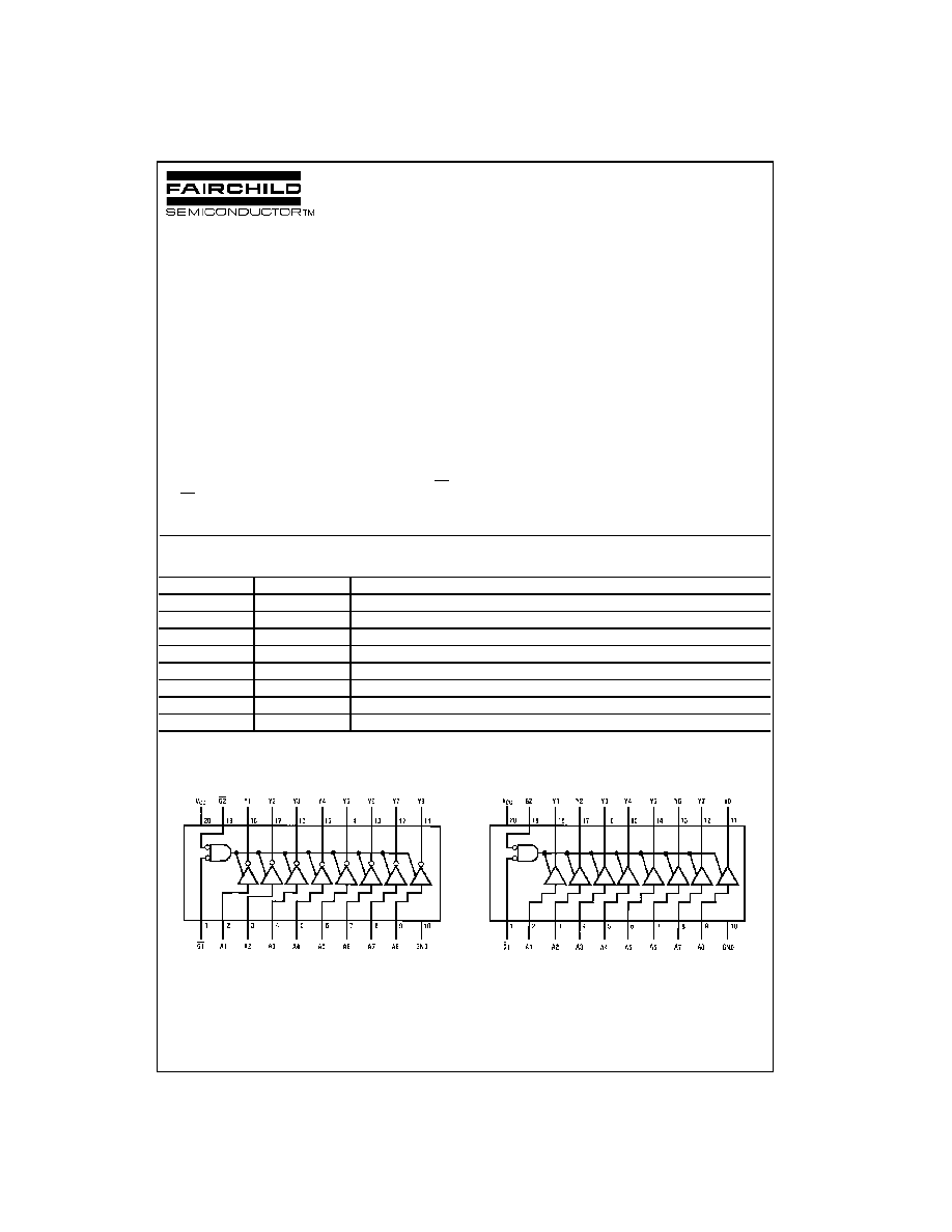
The MM74HC540 is an inverting buffer and the
MM74HC541 is a non-inverting buffer. The 3-STATE con-
trol gate operates as a two-input NOR such that if either G1
or G2 are HIGH, all eight outputs are in the high-imped-
ance state.
In order to enhance PC board layout, the MM74HC540 and
MM74HC541 offers a pinout having inputs and outputs on
opposite sides of the package. All inputs are protected from
damage due to static discharge by diodes to V
CC
and
ground.
Features
s
Typical propagation delay: 12 ns
s
3-STATE outputs for connection to system buses
s
Wide power supply range: 2≠6V
s
Low quiescent current: 80
µ
A maximum (74HC Series)
s
Output current: 6 mA
Ordering Code:
Devices also available in Tape and Reel. Specify by appending the suffix letter "X" to the ordering code.
Connection Diagrams
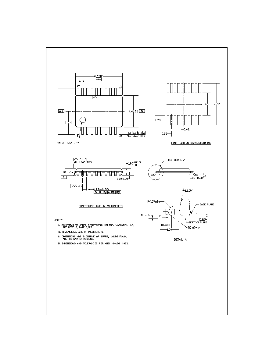
Pin Assignments for DIP, SOIC, SOP and TSSOP
Top View
MM74HC540
Top View
MM74HC541
Order Number
Package Number
Package Description
MM74HC540WM
M20B
20-Lead Small Outline Integrated Circuit (SOIC), JEDEC MS-013, 0.300" Wide
MM74HC540SJ
M20D
20-Lead Small Outline Package (SOP), EIAJ TYPE II, 5.3mm Wide
MM74HC540MTC
MTC20
20-Lead Thin Shrink Small Outline Package (TSSOP), JEDEC MO-153, 4.4mm Wide
MM74HC540N
N20A
20-Lead Plastic Dual-In-Line Package (PDIP), JEDEC MS-001, 0.300" Wide
MM74HC541WM
M20B
20-Lead Small Outline Integrated Circuit (SOIC), JEDEC MS-013, 0.300" Wide
MM74HC541SJ
M20D
20-Lead Small Outline Package (SOP), EIAJ TYPE II, 5.3mm Wide
MM74HC541MTC
MTC20
20-Lead Thin Shrink Small Outline Package (TSSOP), JEDEC MO-153, 4.4mm Wide
MM74HC541N
N20A
20-Lead Plastic Dual-In-Line Package (PDIP), JEDEC MS-001, 0.300" Wide

www.fairchildsemi.com
2
MM74HC540
∑ MM
74HC541
Absolute Maximum Ratings
(Note 1)
(Note 2)
Recommended Operating
Conditions
Note 1: Absolute Maximum Ratings are those values beyond which dam-
age to the device may occur.
Note 2: Unless otherwise specified all voltages are referenced to ground.
Note 3: Power Dissipation temperature derating -- plastic "N" package:
-
12 mW/
∞
C from 65
∞
C to 85
∞
C.
DC Electrical Characteristics
(Note 4)
Note 4: For a power supply of 5V
±
10% the worst case output voltages (V
OH
, and V
OL
) occur for HC at 4.5V. Thus the 4.5V values should be used when
designing with this supply. Worst case V
IH
and V
IL
occur at V
CC
=
5.5V and 4.5V respectively. (The V
IH
value at 5.5V is 3.85V.) The worst case leakage cur-
rent (I
IN
, I
CC
, and I
OZ
) occur for CMOS at the higher voltage and so the 6.0V values should be used.
Supply Voltage (V
CC
)
-
0.5 to
+
7.0V
DC Input Voltage (V
IN
)
-
1.5 to V
CC
+
1.5V
DC Output Voltage (V
OUT
)
-
0.5 to V
CC
+
0.5V
Clamp Diode Current (I
CD
)
±
20 mA
DC Output Current, per pin (I
OUT
)
±
35 mA
DC V
CC
or GND Current,
per pin (I
CC
)
±
70 mA
Storage Temperature Range (T
STG
)
-
65
∞
C to
+
150
∞
C
Power Dissipation (P
D
)
(Note 3)
600 mW
S.O. Package only
500 mW
Lead Temperature (T
L
)
(Soldering 10 seconds)
260
∞
C
Min
Max
Units
Supply Voltage (V
CC
)
2
6
V
DC Input or Output Voltage
(V
IN
, V
OUT
)
0
V
CC
V
Operating Temperature Range (T
A
)
-
40
+
85
∞
C
Input Rise or Fall Times
(t
r
, t
f
) V
CC
=
2.0V
1000
ns
V
CC
=
4.5V
500
ns
V
CC
=
6.0V
400
ns
Symbol
Parameter
Conditions
V
CC
T
A
=
25
∞
C
T
A
=
-
40 to 85
∞
C T
A
=
-
55 to 125
∞
C
Units
Typ
Guaranteed Limits
V
IH
Minimum HIGH Level
2.0V
1.5
1.5
1.5
V
Input Voltage
4.5V
3.15
3.15
3.15
V
6.0V
4.2
4.2
4.2
V
V
IL
Maximum LOW Level
2.0V
0.5
0.5
0.5
V
Input Voltage
4.5V
1.35
1.35
1.35
V
6.0V
1.8
1.8
1.8
V
V
OH
Minimum HIGH Level
V
IN
=
V
IH
or V
IL
Output Voltage
|I
OUT
|
20
µ
A
2.0V
2.0
1.9
1.9
1.9
V
4.5V
4.5
4.4
4.4
4.4
V
6.0V
6.0
5.9
5.9
5.9
V
V
IN
=
V
IH
or V
IL
|I
OUT
|
6.0 mA
4.5V
4.2
3.98
3.84
3.7
V
|I
OUT
|
7.8 mA
6.0V
5.7
5.48
5.34
5.2
V
V
OL
Maximum LOW Level
V
IN
=
V
IH
or V
IL
Output Voltage
|I
OUT
|
20
µ
A
2.0V
0
0.1
0.1
0.1
V
4.5V
0
0.1
0.1
0.1
V
6.0V
0
0.1
0.1
0.1
V
V
IN
=
V
IH
or V
IL
|I
OUT
|
6.0 mA
4.5V
0.2
0.26
0.33
0.4
V
|I
OUT
|
7.8 mA
6.0V
0.2
0.26
0.33
0.4
V
I
IN
Maximum Input
V
IN
=
V
CC
or GND
6.0V
±
0.1
±
1.0
±
1.0
µ
A
Current
I
OZ
Maximum 3-STATE
V
IN
=
V
IH
or V
IL
, G
=
V
IH
6.0V
±
0.5
±
5
±
10
µ
A
Output Leakage
V
OUT
=
V
CC
or GND
Current
I
CC
Maximum Quiescent
V
IN
=
V
CC
or GND
6.0V
8.0
80
160
µ
A
Supply Current
I
OUT
=
0
µ
A

3
www.fairchildsemi.com
MM74HC540
∑ MM74HC541
AC Electrical Characteristics
V
CC
=
5V, T
A
=
25
∞
C, t
r
=
t
f
=
6 ns
AC Electrical Characteristics
V
CC
=
2.0V to 6.0V, C
L
=
50 pF, t
r
=
t
f
=
6 ns (unless otherwise specified)
Note 5: C
PD
determines the no load dynamic power consumption, P
D
=
C
PD
V
CC
2
f
+
I
CC
V
CC
, and the no load dynamic current consumption,
I
S
=
C
PD
V
CC
f
+
I
CC
.
Symbol
Parameter
Conditions
Typ
Guaranteed
Units
Limit
t
PHL
, t
PLH
Maximum Propagation
C
L
=
45 pF
12
18
ns
Delay (540)
t
PHL
, t
PLH
Maximum Propagation
C
L
=
45 pF
14
20
ns
Delay (541)
t
PZH
, t
PZL
Maximum Output Enable
R
L
=
1 k
17
28
ns
Time
C
L
=
45 pF
t
PHZ
, t
PLZ
Maximum Output Disable
R
L
=
1 k
15
25
ns
Time
C
L
=
5 pF
Symbol
Parameter
Conditions
V
CC
T
A
=
25
∞
C
T
A
=
-
40 to 85
∞
C T
A
=
-
55 to 125
∞
C
Units
Typ
Guaranteed Limits
t
PHL
, t
PLH
Maximum Propagation
C
L
=
50 pF
2.0V
55
100
126
149
ns
Delay (540)
C
L
=
150 pF
2.0V
83
150
190
224
ns
C
L
=
50 pF
4.5V
12
20
25
30
ns
C
L
=
150 pF
4.5V
22
30
38
45
ns
C
L
=
50 pF
6.0V
11
17
21
25
ns
C
L
=
150 pF
6.0V
18
26
32
38
ns
t
PHL
, t
PLH
Maximum Propagation
C
L
=
50 pF
2.0V
58
115
145
171
ns
Delay (541)
C
L
=
150 pF
2.0V
83
165
208
246
ns
C
L
=
50 pF
4.5V
14
23
29
34
ns
C
L
=
150 pF
4.5V
17
33
42
49
ns
C
L
=
50 pF
6.0V
11
20
25
29
ns
C
L
=
150 pF
6.0V
14
28
35
42
ns
t
PZH
, t
PZL
Maximum Output Enable
R
L
=
1 k
Time
C
L
=
50 pF
2.0V
75
150
189
224
ns
C
L
=
150 pF
2.0V
100
200
252
298
ns
C
L
=
50 pF
4.5V
15
30
38
45
ns
C
L
=
150 pF
4.5V
30
40
50
60
ns
C
L
=
50 pF
6.0V
13
26
32
38
ns
C
L
=
150 pF
6.0V
17
34
43
51
ns
t
PHZ
, t
PLZ
Maximum Output Disable
R
L
=
1 k
2.0V
75
150
189
224
ns
Time
C
L
=
50 pF
4.5V
15
30
38
45
ns
6.0V
13
26
32
38
ns
t
THL
, t
TLH
Maximum Output Rise
C
L
=
50 pF
2.0V
25
60
75
90
ns
and Fall Time
4.5V
7
12
15
18
ns
6.0V
6
10
13
15
ns
C
PD
Power Dissipation
G
=
V
IH
10
pF
Capacitance (Note 5)
G
=
V
IL
50
pF
C
IN
Maximum Input
5
10
10
10
pF
Capacitance
C
OUT
Maximum Output Capacitance
15
20
20
20
pF