 | –≠–ª–µ–∫—Ç—Ä–æ–Ω–Ω—ã–π –∫–æ–º–ø–æ–Ω–µ–Ω—Ç: 74LCX00 | –°–∫–∞—á–∞—Ç—å:  PDF PDF  ZIP ZIP |
March 1995
Revised March 1999
7
4LCX00 Low
V
o
l
t
age Quad
2-I
nput
NAND Gat
e
wi
th
5V T
o
l
e
rant
Input
s
© 1999 Fairchild Semiconductor Corporation
DS012408.prf
www.fairchildsemi.com
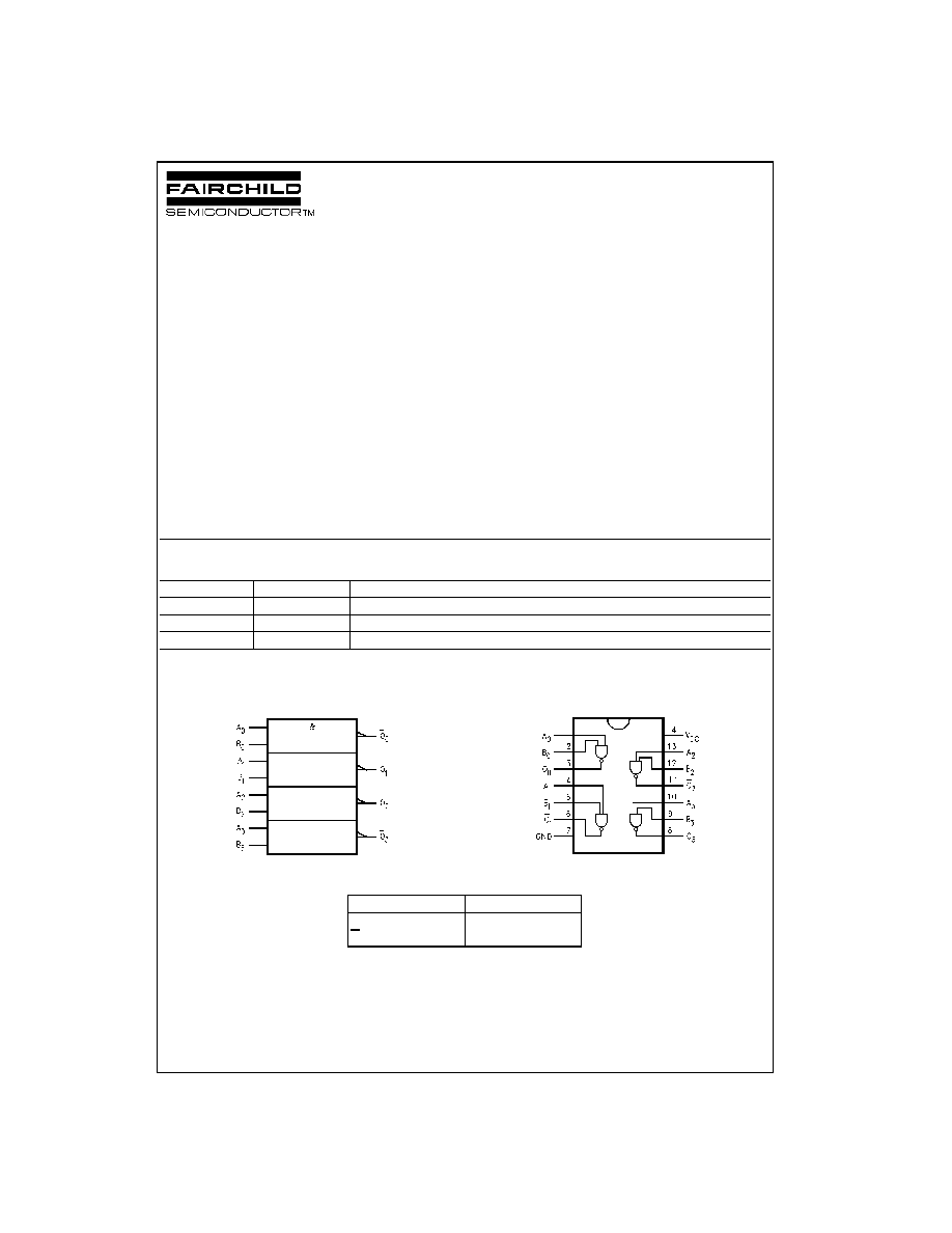
74LCX00
Low Voltage Quad 2-Input NAND Gate with 5V Tolerant
Inputs
General Description
The LCX00 contains four 2-input NAND gates. The inputs
tolerate voltages up to 7V allowing the interface of 5V sys-
tems to 3V systems.
The 74LCX00 is fabricated with advanced CMOS technol-
ogy to achieve high speed operation while maintaining
CMOS low power dissipation.
Features
s
5V tolerant inputs
s
2.3V≠3.6V V
CC
specifications provided
s
5.2 ns t
PD
max (V
CC
=
3.3V), 10
µ
A I
CC
max
s
Power down high impedance inputs and outputs
s
±
24 mA output drive (V
CC
=
3.0V)
s
Implements patented noise/EMI reduction circuitry
s
Latch-up performance exceeds 500 mA
s
ESD performance:
Human body model
>
2000V
Machine model
>
200V
Ordering Code:
Devices also available in Tape and Reel. Specify by appending the suffix letter "X" to the ordering code.
Logic Symbol
IEEE/IEC
Connection Diagram
Pin Descriptions
Order Number
Package Number
Package Description
74LCX00M
M14A
14-Lead Small Outline Integrated Circuit (SOIC), JEDEC MS-120, 0.150" Narrow
74LCX00SJ
M14D
14-Lead Small Outline Package (SOP), EIAJ TYPE II, 5.3mm Wide
74LCX00MTC
MTC14
14-Lead Thin Shrink Small Outline Package (TSSOP), JEDEC MO-153, 4.4mm Wide
Pin Names
Description
A
n
, B
n
Inputs
O
n
Outputs
www.fairchildsemi.com
2
74L
C
X
00
Absolute Maximum Ratings
(Note 1)
Recommended Operating Conditions
(Note 3)
Note 1: The Absolute Maximum Ratings are those values beyond which the safety of the device cannot be guaranteed. The device should not be operated
at these limits. The parametric values defined in the Electrical Characteristics tables are not guaranteed at the Absolute Maximum Ratings. The "Recom-
mended Operating Conditions" table will define the conditions for actual device operation.
Note 2: I
O
Absolute Maximum Rating must be observed.
Note 3: Unused inputs must be held HIGH or LOW. They may not float.
DC Electrical Characteristics
Symbol
Parameter
Value
Conditions
Units
V
CC
Supply Voltage
-
0.5 to
+
7.0
V
V
I
DC Input Voltage
-
0.5 to
+
7.0
V
V
O
DC Output Voltage
-
0.5 to V
CC
+
0.5
Output in HIGH or LOW State (Note 2)
V
I
IK
DC Input Diode Current
-
50
V
I
<
GND
mA
I
OK
DC Output Diode Current
-
50
V
O
<
GND
mA
+
50
V
O
>
V
CC
I
O
DC Output Source/Sink Current
±
50
mA
I
CC
DC Supply Current per Supply Pin
±
100
mA
I
GND
DC Ground Current per Ground Pin
±
100
mA
T
STG
Storage Temperature
-
65 to
+
150
∞
C
Symbol
Parameter
Min
Max
Units
V
CC
Supply Voltage
Operating
2.0
3.6
V
Data Retention
1.5
3.6
V
I
Input Voltage
0
5.5
V
V
O
Output Voltage
HIGH or LOW State
0
V
CC
V
I
OH
/I
OL
Output Current
V
CC
=
3.0V
-
3.6V
±
24
mA
V
CC
=
2.7V - 3.0V
±
12
V
CC
=
2.3V - 2.7V
±
8
T
A
Free-Air Operating Temperature
-
40
85
∞
C
t/
V
Input Edge Rate, V
IN
=
0.8V≠2.0V, V
CC
=
3.0V
0
10
ns/V
Symbol
Parameter
Conditions
V
CC
T
A
=
-
40
∞
C to
+
85
∞
C
Units
(V)
Min
Max
V
IH
HIGH Level Input Voltage
2.3
-
2.7
1.7
V
2.7
-
3.6
2.0
V
IL
LOW Level Input Voltage
2.3
-
2.7
0.7
V
2.7
-
3.6
0.8
V
OH
HIGH Level Output Voltage
I
OH
=
-
100
µ
A
2.3
-
3.6
V
CC
-
0.2
V
I
OH
=
-
8 mA
2.3
1.8
I
OH
=
-
12 mA
2.7
2.2
I
OH
=
-
18 mA
3.0
2.4
I
OH
=
-
24 mA
3.0
2.2
V
OL
LOW Level Output Voltage
I
OL
=
100
µ
A
2.3
-
3.6
0.2
V
I
OL
=
8mA
2.3
0.6
I
OL
=
12 mA
2.7
0.4
I
OL
=
16 mA
3.0
0.4
I
OL
=
24 mA
3.0
0.55
I
I
Input Leakage Current
0
V
I
5.5V
2.3
-
3.6
±
5.0
µ
A
I
OFF
Power-Off Leakage Current
V
I
or V
O
=
5.5V
0
10
µ
A
I
CC
Quiescent Supply Current
V
I
=
V
CC
or GND
2.3
-
3.6
10
µ
A
3.6V
V
I
5.5V
2.3
-
3.6
±
10
I
CC
Increase in I
CC
per Input
V
IH
=
V
CC
-
0.6V
2.3
-
3.6
500
µ
A
3
www.fairchildsemi.com
7
4LCX00
AC Electrical Characteristics
Note 4: Skew is defined as the absolute value of the difference between the actual propagation delay for any two separate outputs of the same device. The
specification applies to any outputs switching in the same direction, either HIGH-to-LOW (t
OSHL
) or LOW-to-HIGH (t
OSLH
).
Dynamic Switching Characteristics
Capacitance
Symbol
Parameter
T
A
=
-
40
∞
C to
+
85
∞
CF, R
L
=
500
Units
V
CC
=
3.3V
±
0.3V
V
CC
=
2.7V
V
CC
=
2.5V
±
0.2V
C
L
=
50pF
C
L
=
50pF
C
L
=
30pF
Min
Max
Min
Max
Min
Max
t
PHL
Propagation Delay
1.5
5.2
1.5
6.0
1.5
6.2
ns
t
PLH
1.5
5.2
1.5
6.0
1.5
6.2
t
OSHL
Output to Output Skew (Note 4)
1.0
ns
t
OSLH
1.0
Symbol
Parameter
Conditions
V
CC
(V)
T
A
=
25
∞
C
Unit
Typical
V
OLP
Quiet Output Dynamic Peak V
OL
C
L
=
50 pF, V
IH
=
3.3V, V
IL
=
0V
3.3
0.8
V
C
L
=
30 pF, V
IH
=
2.5V, V
IL
=
0V
2.5
0.6
V
OLV
Quiet Output Dynamic Valley V
OL
C
L
=
50 pF, V
IH
=
3.3V, V
IL
=
0V
3.3
-
0.8
V
C
L
=
30 pF, V
IH
=
2.5V, V
IL
=
0V
2.5
-
0.6
Symbol
Parameter
Conditions
Typical
Units
C
IN
Input Capacitance
V
CC
=
Open, V
I
=
0V or V
CC
7
pF
C
OUT
Output Capacitance
V
CC
=
3.3V, V
I
=
0V or V
CC
8
pF
C
PD
Power Dissipation Capacitance
V
CC
=
3.3V, V
I
=
0V or V
CC
, f
=
10 MHz
25
pF
www.fairchildsemi.com
4
74L
C
X
00
AC LOADING and WAVEFORMS
Generic for LCX Family
FIGURE 1. AC Test Circuit (C
L
includes probe and jig capacitance)
Waveform for Inverting and Non-Inverting Functions
Propagation Delay. Pulse Width and t
rec
Waveforms
3-STATE Output Low Enable and
Disable Times for Logic
3-STATE Output High Enable and
Disable Times for Logic
Setup Time, Hold Time and Recovery Time for Logic
t
rise
and t
fall
FIGURE 2. Waveforms
(Input Characteristics; f =1MHz, t
R
= t
F
= 3ns)
Test
Switch
t
PLH
, t
PHL
Open
t
PZL
, t
PLZ
6V at V
CC
=
3.3
±
0.3V
V
CC
x 2 at V
CC
=
2.5
±
0.2V
t
PZH
,t
PHZ
GND
Symbol
V
CC
3.3V
±
0.3V
2.7V
2.5V
±
0.2V
V
mi
1.5V
1.5V
V
CC
/2
V
mo
1.5V
1.5V
V
CC
/2
V
x
V
OL
+
0.3V
V
OL
+
0.3V
V
OL
+
0.15V
V
y
V
OH
-
0.3V
V
OH
-
0.3V
V
OH
-
0.15V
5
www.fairchildsemi.com
7
4LCX00
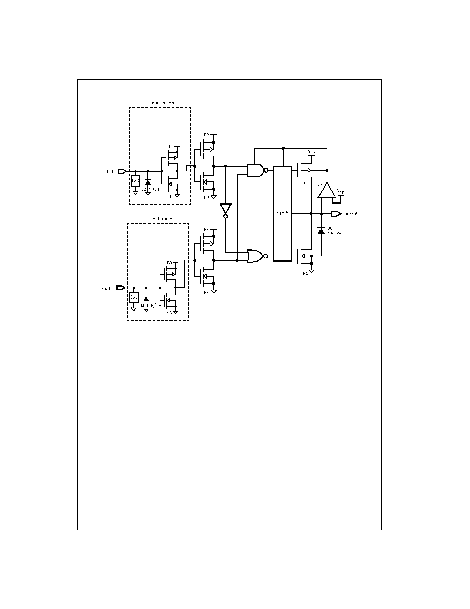
Schematic Diagram
Generic for LCX Family