 | –≠–ª–µ–∫—Ç—Ä–æ–Ω–Ω—ã–π –∫–æ–º–ø–æ–Ω–µ–Ω—Ç: 74LCX11 | –°–∫–∞—á–∞—Ç—å:  PDF PDF  ZIP ZIP |
© 2005 Fairchild Semiconductor Corporation
DS012426
www.fairchildsemi.com
April 1995
Revised July 2005
7
4LCX1
1
Low V
o
l
t
age T
r
i
p
l
e
3-
Inpu
t A
ND Gate wit
h
5V T
o
ler
ant I
nput
s
74LCX11
Low Voltage Triple 3-Input AND Gate
with 5V Tolerant Inputs
General Description
The LCX11 is a triple 3-input AND gate with buffered out-
puts. LCX devices are designed for low voltage (2.5V or
3.3V) operation with the added capability of interfacing to a
5V signal environment.
The 74LCX11 is fabricated with advanced CMOS technol-
ogy to achieve high speed operation while maintaining
CMOS low power dissipation.
Features
s
5V tolerant inputs and outputs
s
2.3V≠3.6V V
CC
specifications provided
s
6.0ns t
PD
max (V
CC
3.3V), 10
P
A I
CC
max
s
Power down high impedance inputs and outputs
s
r
24 mA output drive (V
CC
3.0V)
s
Implements patented noise/EMI reduction circuitry
s
Latch-up performance exceeds JEDEC 78 conditions
s
ESD performance:
Human body model
!
2000V
Machine model
!
200V
s
Leadless DQFN Package
Ordering Code:
Pb-Free package per JEDEC J-STD-020B.
Note 1: "_NL" indicates Pb-Free package (per JEDEC J-STD-020B). Device available in Tape and Reel only.
Note 2: DQFN package available in Tape and Reel only.
Order Number
Package
Package Description
Number
74LCX11M
M14A
14-Lead Small Outline Integrated Circuit (SOIC), JEDEC MS-012, 0.150" Narrow
74LCX11MX_NL
(Note 1)
M14A
Pb-Free 14-Lead Small Outline Integrated Circuit (SOIC), JEDEC MS-012, 0.150" Narrow
74LCX11SJ
M14D
14-Lead Small Outline Package (SOP), EIAJ TYPE II, 5.3mm Wide
74LCX11BQX
(Note 2)
MLP014A
Pb-Free 14-Terminal Depopulated Quad Very-Thin Flat Pack No Leads (DQFN), JEDEC
MO-241, 2.5 x 3.0mm
74LCX11MTC
MTC14
14-Lead Thin Shrink Small Outline Package (TSSOP), JEDEC MO-153, 4.4mm Wide
74LCX11MTCX_NL
(Note 1)
MTC14
Pb-Free 14-Lead Thin Shrink Small Outline Package (TSSOP), JEDEC MO-153, 4.4mm
Wide
www.fairchildsemi.com
2
74L
C
X
1
1
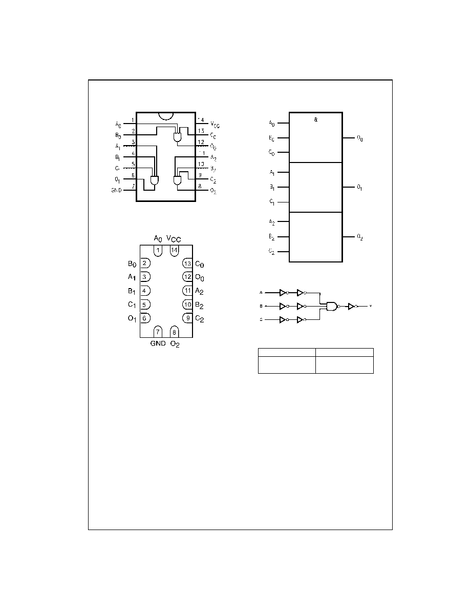
Connection Diagrams
Pin Assignments for SOIC, SOP, and TSSOP
(Top View)
Pad Assignments for DQFN
(Top Through View)
Logic Symbol
IEEE/IEC
Logic Diagram
Pin Descriptions
Pin Names
Description
A
n
, B
n
, C
n
Inputs
O
n
Outputs
3
www.fairchildsemi.com
7
4LCX1
1
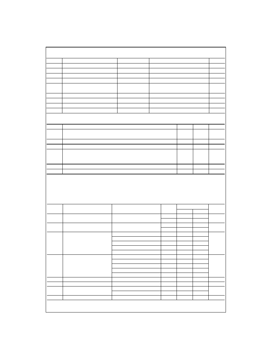
Absolute Maximum Ratings
(Note 3)
Recommended Operating Conditions
(Note 5)
Note 3: The Absolute Maximum Ratings are those values beyond which the safety of the device cannot be guaranteed. The device should not be operated
at these limits. The parametric values defined in the Electrical Characteristics tables are not guaranteed at the Absolute Maximum Ratings. The "Recom-
mended Operating Conditions" table will define the conditions for actual device operation.
Note 4: I
O
Absolute Maximum Rating must be observed.
Note 5: Unused inputs must be held HIGH or LOW. They may not float.
DC Electrical Characteristics
Symbol
Parameter
Value
Conditions
Units
V
CC
Supply Voltage
0.5 to
7.0
V
V
I
DC Input Voltage
0.5 to
7.0
V
V
O
DC Output Voltage
0.5 to V
CC
0.5
Output in HIGH or LOW State (Note 4)
V
I
IK
DC Input Diode Current
50
V
I
GND
mA
I
OK
DC Output Diode Current
50
V
O
GND
mA
50
V
O
!
V
CC
I
O
DC Output Source/Sink Current
r
50
mA
I
CC
DC Supply Current per Supply Pin
r
100
mA
I
GND
DC Ground Current per Ground Pin
r
100
mA
T
STG
Storage Temperature
65 to
150
q
C
Symbol
Parameter
Min
Max
Units
V
CC
Supply Voltage
Operating
2.0
3.6
V
Data Retention
1.5
3.6
V
I
Input Voltage
0
5.5
V
V
O
Output Voltage
HIGH or LOW State
0
V
CC
V
I
OH
/I
OL
Output Current
V
CC
3.0V
3.6V
r
24
mA
V
CC
2.7V
3.0V
r
12
V
CC
2.3V
2.7V
r
8
T
A
Free-Air Operating Temperature
40
85
q
C
'
t/
'
V
Input Edge Rate, V
IN
0.8V≠2.0V, V
CC
3.0V
0
10
ns/V
Symbol
Parameter
Conditions
V
CC
T
A
40
q
C to
85
q
C
Units
(V)
Min
Max
V
IH
HIGH Level Input Voltage
2.3
2.7
1.7
V
2.7
3.6
2.0
V
IL
LOW Level Input Voltage
2.3
2.7
0.7
V
2.7
3.6
0.8
V
OH
HIGH Level Output Voltage
I
OH
100
P
A
2.3
3.6
V
CC
0.2
V
I
OH
8 mA
2.3
1.8
I
OH
12mA
2.7
2.2
I
OH
18mA
3.0
2.4
I
OH
24mA
3.0
2.2
V
OL
LOW Level Output Voltage
I
OL
100
P
A
2.3
3.6
0.2
V
I
OL
8 mA
2.3
0.6
I
OL
12mA
2.7
0.4
I
OL
16 mA
3.0
0.4
I
OL
24 mA
3.0
0.55
I
I
Input Leakage Current
0
d
V
I
d
5.5V
2.3
3.6
r
5.0
P
A
I
OFF
Power-Off Leakage Current
V
I
or V
O
5.5V
0
10
P
A
I
CC
Quiescent Supply Current
V
I
V
CC
or GND
2.3
3.6
10
P
A
3.6V
d
V
I
d
5.5V
2.3
3.6
r
10
'
I
CC
Increase in I
CC
per Input
V
IH
V
CC
0.6V
2.3
3.6
500
P
A
www.fairchildsemi.com
4
74L
C
X
1
1
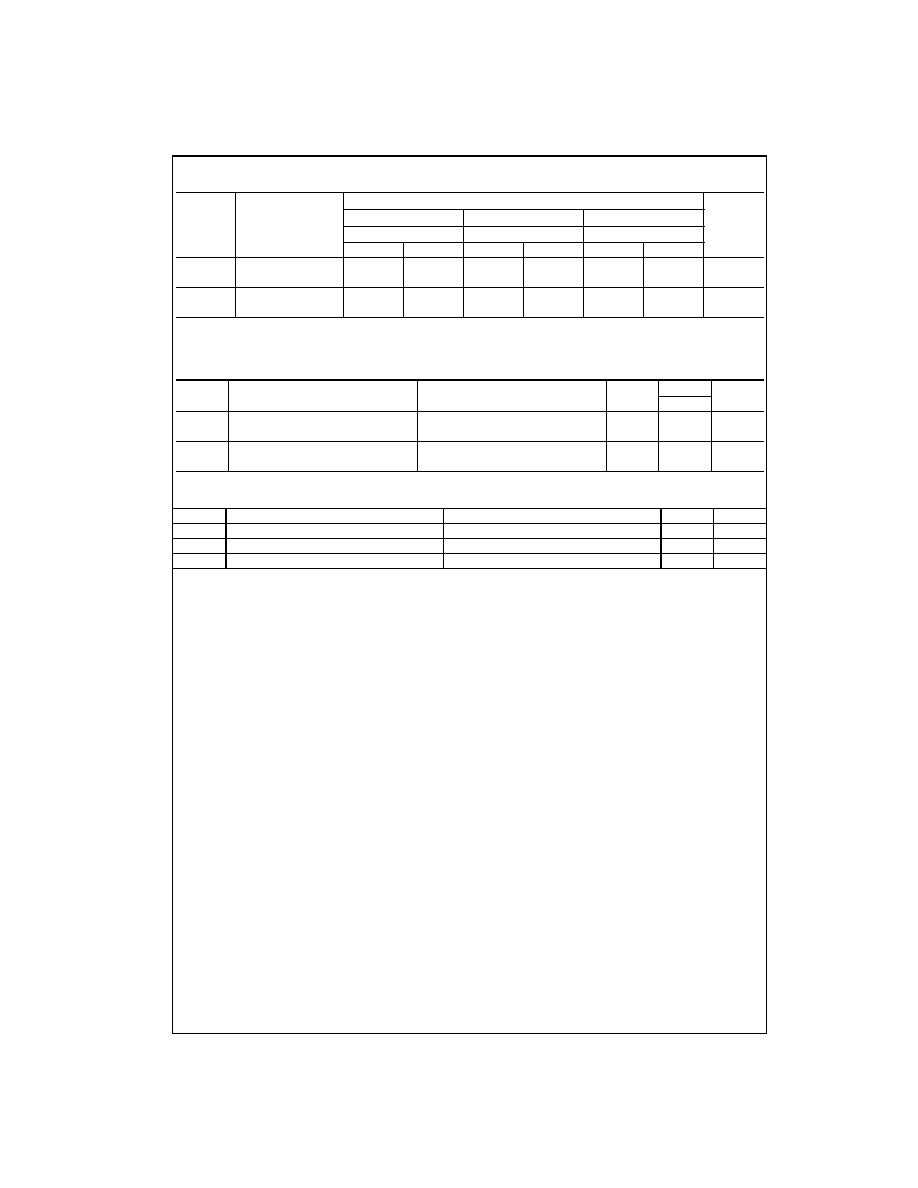
AC Electrical Characteristics
Note 6: Skew is defined as the absolute value of the difference between the actual propagation delay for any two separate outputs of the same device. The
specification applies to any outputs switching in the same direction, either HIGH-to-LOW (t
OSHL
) or LOW-to-HIGH (t
OSLH
).
Dynamic Switching Characteristics
Capacitance
Symbol
Parameter
T
A
40
q
C to
85
q
C, R
L
500
:
Units
V
CC
3.3V
r
0.3V
V
CC
2.7V
V
CC
2.5V
r
0.2V
C
L
50 pF
C
L
50 pF
C
L
30pF
Min
Max
Min
Max
Min
Max
t
PLH
Propagation Delay
1.5
6.0
1.5
7.0
1.5
7.2
ns
t
PHL
1.5
6.0
1.5
7.0
1.5
7.2
t
OSLH
Output to Output Skew
1.0
ns
t
OSHL
(Note 6)
1.0
Symbol
Parameter
Conditions
V
CC
T
A
25
q
C
Units
(V)
Typical
V
OLP
Quiet Output Dynamic Peak V
OL
C
L
50 pF, V
IH
3.3V, V
IL
0V
3.3
0.8
V
C
L
30 pF, V
IH
2.5V, V
IL
0V
2.5
0.6
V
OLV
Quiet Output Dynamic Peak V
OL
C
L
50 pF, V
IH
3.3V, V
IL
0V
3.3
0.8
V
C
L
30 pF, V
IH
2.5V, V
IL
0V
2.5
0.6
Symbol
Parameter
Conditions
Typical
Units
C
IN
Input Capacitance
V
CC
Open, V
I
0V or V
CC
7
pF
C
OUT
Output Capacitance
V
CC
3.3V, V
I
0V or V
CC
8
pF
C
PD
Power Dissipation Capacitance
V
CC
3.3V, V
I
0V or V
CC
, f
10 MHz
25
pF
5
www.fairchildsemi.com
7
4LCX1
1
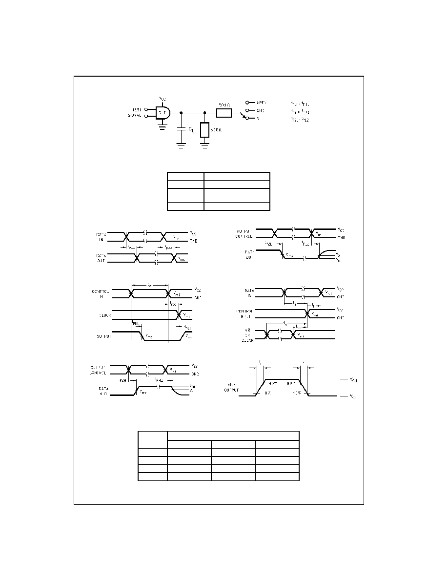
AC Loading and Waveforms
Generic for LCX Family
FIGURE 1. AC Test Circuit
(C
L
includes probe and jig capacitance)
Waveform for Inverting and Non-Inverting Functions
Propagation Delay, Pulse Width and t
rec
Waveforms
3-STATE Output High Enable and
Disable TImes for Logic
3-STATE Output Low Enable and
Disable Times for Logic
Setup Time, Hold TIme and Recovery TIme for Logic
t
rise
and t
fall
FIGURE 2. Waveforms
(Input Pulse Characteristics; f = 1MHz, t
r
= t
f
= 3ns)
Test
Switch
t
PLH
, t
PHL
Open
t
PZL
, t
PLZ
6V at V
CC
3.3
r
0.3V
V
CC
x 2 at V
CC
2.5
r
0.2V
t
PZH
, t
PHZ
GND
Symbol
V
CC
3.3V
r
0.3V
2.7V
2.5V
r
0.2V
V
mi
1.5V
1.5V
V
CC
/2
V
mo
1.5V
1.5V
V
CC
/2
V
x
V
OL
0.3V
V
OL
0.3V
V
OL
0.15V
V
y
V
OH
0.3V
V
OH
0.3V
V
OH
0.15V
www.fairchildsemi.com
6
74L
C
X
1
1
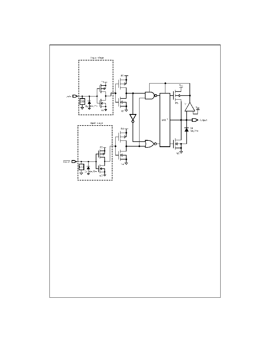
Schematic Diagram
Generic for LCX Family
7
www.fairchildsemi.com
7
4LCX1
1
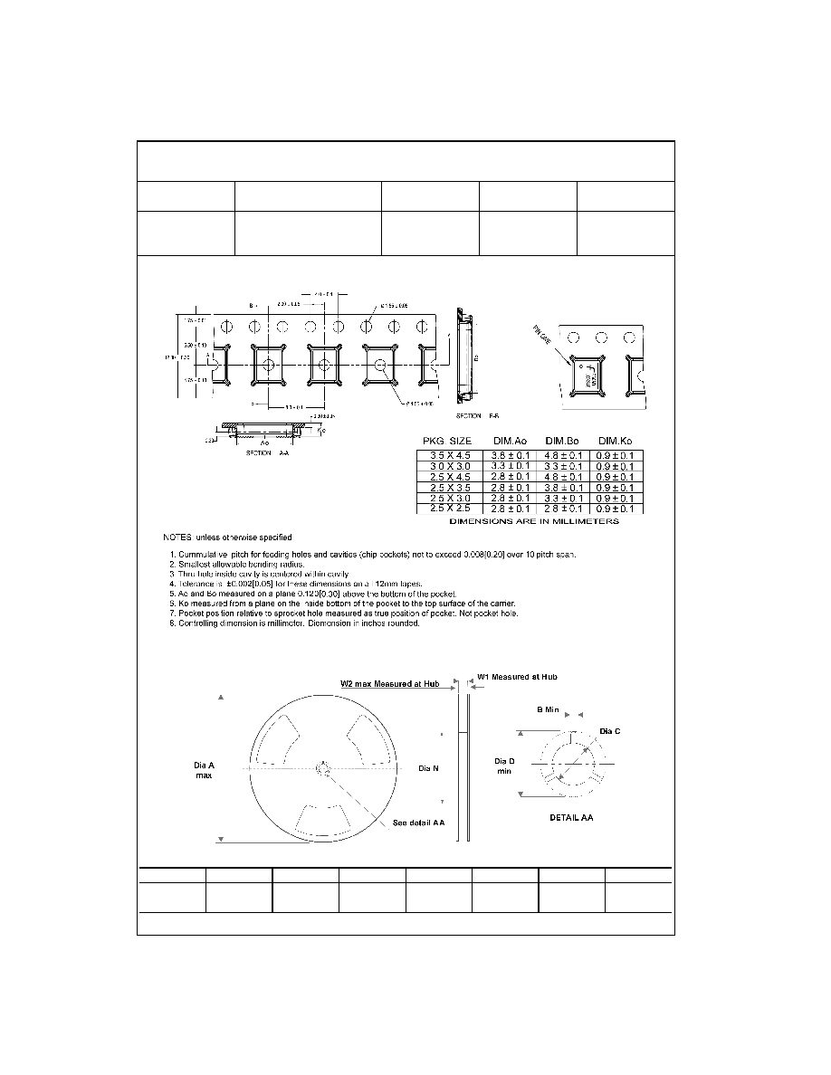
Tape and Reel Specification
Tape Format for DQFN
TAPE DIMENSIONS inches (millimeters)
REEL DIMENSIONS inches (millimeters)
Package
Tape
Number
Cavity
Cover Tape
Designator
Section
Cavities
Status
Status
Leader (Start End)
125 (typ)
Empty
Sealed
BQX
Carrier
3000
Filled
Sealed
Trailer (Hub End)
75 (typ)
Empty
Sealed
Tape Size
A
B
C
D
N
W1
W2
12 mm
13.0
0.059
0.512
0.795
2.165
0.488
0.724
(330.0)
(1.50)
(13.00)
(20.20)
(55.00)
(12.4)
(18.4)
www.fairchildsemi.com
8
74L
C
X
1
1
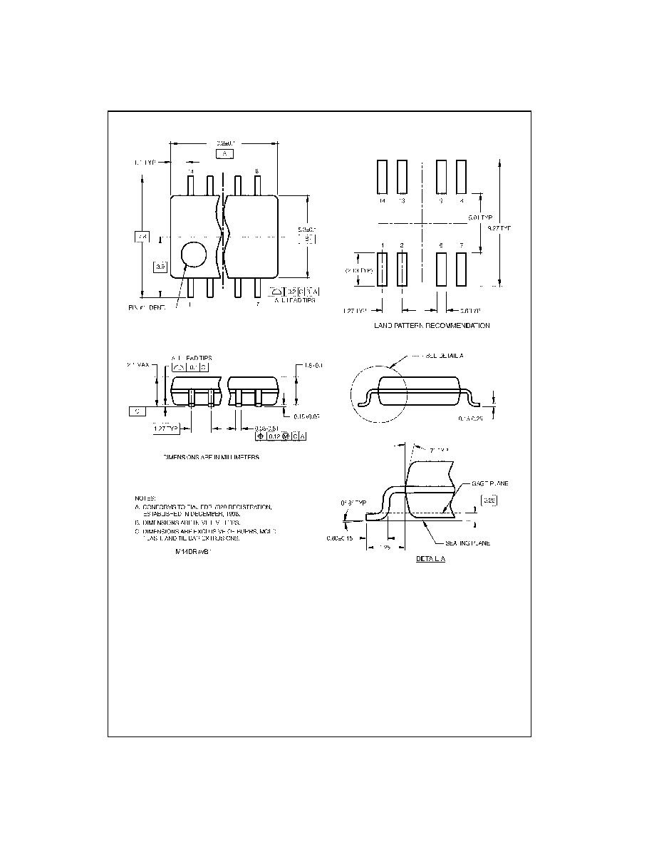
Physical Dimensions
inches (millimeters) unless otherwise noted
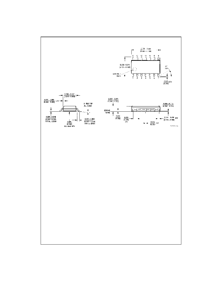
14-Lead Small Outline Integrated Circuit (SOIC), JEDEC MS-012, 0.150" Narrow
Package Number M14A
9
www.fairchildsemi.com
7
4LCX1
1
Physical Dimensions
inches (millimeters) unless otherwise noted (Continued)
14-Lead Small Outline Package (SOP), EIAJ TYPE II, 5.3mm Wide
Package Number M14D
www.fairchildsemi.com
10
74L
C
X
1
1
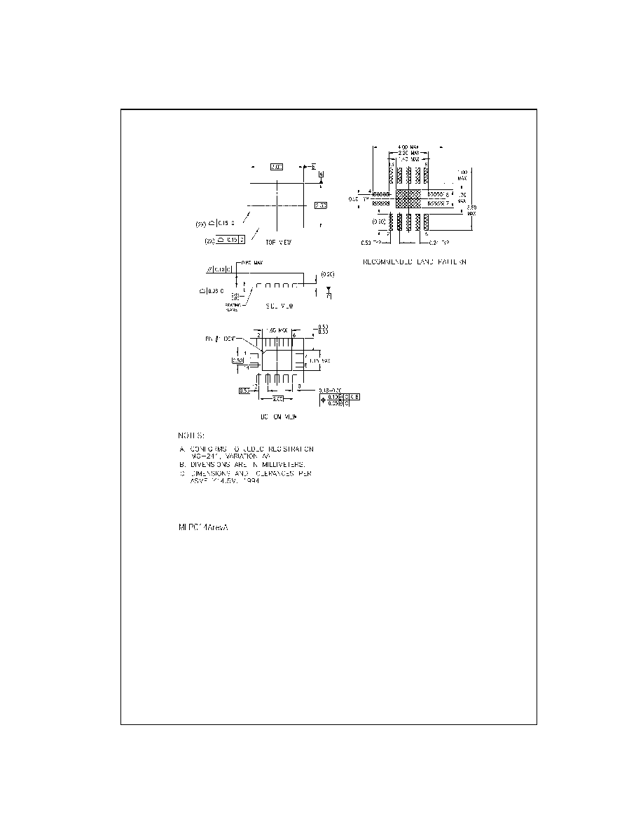
Physical Dimensions
inches (millimeters) unless otherwise noted (Continued)
Pb-Free 14-Terminal Depopulated Quad Very-Thin Flat Pack No Leads (DQFN), JEDEC MO-241, 2.5 x 3.0mm
Package Number MLP014A
11
www.fairchildsemi.com
7
4LCX1
1
Low V
o
l
t
age T
r
i
p
l
e
3-
Inpu
t A
ND Gate wit
h
5V T
o
ler
ant I
nput
s
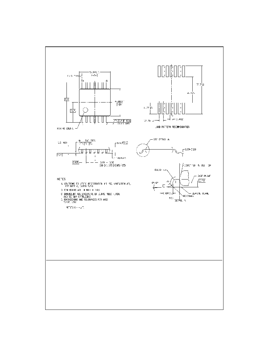
Physical Dimensions
inches (millimeters) unless otherwise noted (Continued)
14-Lead Thin Shrink Small Outline Package (TSSOP), JEDEC MO-153, 4.4mm Wide
Package Number MTC14
Fairchild does not assume any responsibility for use of any circuitry described, no circuit patent licenses are implied and
Fairchild reserves the right at any time without notice to change said circuitry and specifications.
LIFE SUPPORT POLICY
FAIRCHILD'S PRODUCTS ARE NOT AUTHORIZED FOR USE AS CRITICAL COMPONENTS IN LIFE SUPPORT
DEVICES OR SYSTEMS WITHOUT THE EXPRESS WRITTEN APPROVAL OF THE PRESIDENT OF FAIRCHILD
SEMICONDUCTOR CORPORATION. As used herein:
1. Life support devices or systems are devices or systems
which, (a) are intended for surgical implant into the
body, or (b) support or sustain life, and (c) whose failure
to perform when properly used in accordance with
instructions for use provided in the labeling, can be rea-
sonably expected to result in a significant injury to the
user.
2. A critical component in any component of a life support
device or system whose failure to perform can be rea-
sonably expected to cause the failure of the life support
device or system, or to affect its safety or effectiveness.
www.fairchildsemi.com