
© 2001 Fairchild Semiconductor Corporation
DS012465
www.fairchildsemi.com
May 1995
Revised February 2001
7
4
LCX157
Low V
o
lt
age
Quad 2-
Input
Mul
t
i
p
lex
e
r w
i
th 5V T
o
l
e
ra
nt Input
s
74LCX157
Low Voltage Quad 2-Input Multiplexer
with 5V Tolerant Inputs
General Description
The LCX157 is a high-speed quad 2-input multiplexer. Four
bits of data from two sources can be selected using the
common Select and Enable inputs. The four outputs
present the selected data in the true (noninverted) form.
The LCX157 can also be used as a function generator.
The 74LCX157 is fabricated with advanced CMOS technol-
ogy to achieve high speed operation while maintaining
CMOS low power dissipation.
Features
s
5V tolerant inputs
s
2.3V≠3.6V V
CC
specifications provided
s
5.8 ns t
PD
max (V
CC
=
3.3V), 10
µ
A I
CC
max
s
Power down high impedance inputs and outputs
s
±
24 mA output drive (V
CC
=
3.0V)
s
Implements patented noise/EMI reduction circuitry
s
Latch-up performance exceeds 500 mA
s
ESD performance:
Human body model
>
2000V
Machine model
>
200V
Ordering Code:
Devices also available in Tape and Reel. Specify by appending the suffix letter "X" to the ordering code.
Logic Symbols
IEEE/IEC
Connection Diagram
Pin Descriptions
Order Number
Package Number
Package Description
74LCX157M
M16A
16-Lead Small Outline Integrated Circuit (SOIC), JEDEC MS-012, 0.150 Narrow
74LCX157SJ
M16D
16-Lead Small Outline Package (SOP), EIAJ TYPE II, 5.3mm Wide
74LCX157MTC
MTC16
16-Lead Thin Shrink Small Outline Package (TSSOP), JEDEC MO-153, 4.4mm Wide
Pin Names
Description
I
0a
≠I
0d
Source 0 Data Inputs
I
1a
≠I
1d
Source 1 Data Inputs
E
Enable Input
S
Select Input
Z
a
≠Z
d
Outputs
www.fairchildsemi.com
2
74LCX157
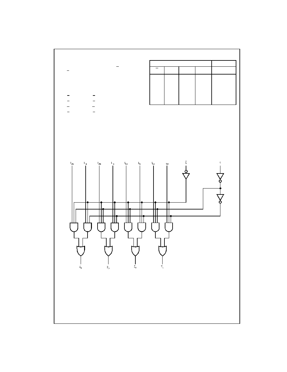
Functional Description
The LCX157 is a quad 2-input multiplexer. It selects four
bits of data from two sources under the control of a com-
mon Select input (S). The Enable input (E) is active-LOW.
When E is HIGH, all of the outputs (Z) are forced LOW
regardless of all other inputs. The LCX157 is the logic
implementation of a 4-pole, 2-position switch where the
position of the switch is determined by the logic levels sup-
plied to the Select input. The logic equations for the outputs
are shown below:
Z
a
=
E ∑ (I
1a
∑ S
+
I
0a
∑ S)
Z
b
=
E ∑ (I
1b
∑ S
+
I
0b
∑ S)
Z
c
=
E ∑ (I
1c
∑ S
+
I
0c
∑ S)
Z
d
=
E ∑ (I
1d
∑ S
+
I
0d
∑ S)
A common use of the LCX157 is the moving of data from
two groups of registers to four common output busses. The
particular register from which the data comes is determined
by the state of the Select input. A less obvious use is as a
function generator. The LCX157 can generate any four of
the sixteen different functions of two variables with one
variable common. This is useful for implementing gating
functions.
Truth Table
H
=
HIGH Voltage Level
L
=
LOW Voltage Level
X
=
Immaterial
Logic Diagram
Please note that this diagram is provided only for the understanding of logic operations and should not be used to estimate propagation delays.
Inputs
Outputs
E
S
I
0
I
1
Z
H
X
X
X
L
L
H
X
L
L
L
H
X
H
H
L
L
L
X
L
L
L
H
X
H

3
www.fairchildsemi.com
7
4
LCX157
Absolute Maximum Ratings
(Note 1)
Recommended Operating Conditions
(Note 3)
Note 1: The Absolute Maximum Ratings are those values beyond which the safety of the device cannot be guaranteed. The device should not be operated
at these limits. The parametric values defined in the Electrical Characteristics tables are not guaranteed at the Absolute Maximum Ratings. The "Recom-
mended Operating Conditions" table will define the conditions for actual device operation.
Note 2: I
O
Absolute Maximum Rating must be observed.
Note 3: Unused inputs must be held HIGH or LOW. They may not float.
DC Electrical Characteristics
Symbol
Parameter
Value
Conditions
Units
V
CC
Supply Voltage
-
0.5 to
+
7.0
V
V
I
DC Input Voltage
-
0.5 to
+
7.0
V
V
O
DC Output Voltage
-
0.5 to V
CC
+
0.5
Output in HIGH or LOW State (Note 2)
V
I
IK
DC Input Diode Current
-
50
V
I
<
GND
mA
I
OK
DC Output Diode Current
-
50
V
O
<
GND
mA
+
50
V
O
>
V
CC
I
O
DC Output Source/Sink Current
±
50
mA
I
CC
DC Supply Current per Supply Pin
±
100
mA
I
GND
DC Ground Current per Ground Pin
±
100
mA
T
STG
Storage Temperature
-
65 to
+
150
∞
C
Symbol
Parameter
Min
Max
Units
V
CC
Supply Voltage
Operating
2.0
3.6
V
Data Retention
1.5
3.6
V
I
Input Voltage
0
5.5
V
V
O
Output Voltage
HIGH or LOW State
0
V
CC
V
I
OH
/I
OL
Output Current
V
CC
=
3.0V
-
3.6V
±
24
mA
V
CC
=
2.7V
-
3.0V
±
12
V
CC
=
2.3V
-
2.7V
±
8
T
A
Free-Air Operating Temperature
-
40
85
∞
C
t/
V
Input Edge Rate, V
IN
=
0.8V
-
2.0V, V
CC
=
3.0V
0
10
ns/V
Symbol
Parameter
Conditions
V
CC
T
A
=
-
40
∞
C to
+
85
∞
C
Units
(V)
Min
Max
V
IH
HIGH Level Input Voltage
2.3
-
2.7
1.7
V
2.7
-
3.6
2.0
V
IL
LOW Level Input Voltage
2.3
-
2.7
0.7
V
2.7
-
3.6
0.8
V
OH
HIGH Level Output Voltage
I
OH
=
-
100
µ
A
2.3
-
3.6
V
CC
-
0.2
V
I
OH
=
-
8 mA
2.3
1.8
I
OH
=
-
12 mA
2.7
2.2
I
OH
=
-
18 mA
3.0
2.4
I
OH
=
-
24 mA
3.0
2.2
V
OL
LOW Level Output Voltage
I
OL
=
100
µ
A
2.3
-
3.6
0.2
V
I
OH
=
8 mA
2.3
0.6
I
OL
=
12 mA
2.7
0.4
I
OL
=
16 mA
3.0
0.4
I
OL
=
24 mA
3.0
0.55
I
I
Input Leakage Current
0
V
I
5.5V
2.3
-
3.6
±
5.0
µ
A
I
OFF
Power-Off Leakage Current
V
I
or V
O
=
5.5V
0
10
µ
A
I
CC
Quiescent Supply Current
V
I
=
V
CC
or GND
2.3
-
3.6
10
µ
A
3.6V
V
I
5.5V
2.3
-
3.6
±
10
I
CC
Increase in I
CC
per Input
V
IH
=
V
CC
-
0.6V
2.3
-
3.6
500
µ
A

www.fairchildsemi.com
4
74LCX157
AC Electrical Characteristics
Note 4: Skew is defined as the absolute value of the difference between the actual propagation delay for any two separate outputs of the same device. The
specification applies to any outputs switching in the same direction, either HIGH-to-LOW (t
OSHL
) or LOW-to-HIGH (t
OSLH
). Parameter guaranteed by design.
Dynamic Switching Characteristics
Capacitance
Symbol
Parameter
T
A
=
-
40
∞
C to
+
85
∞
C, R
L
=
500
Units
V
CC
=
3.3V
±
0.3V
V
CC
=
2.7V
V
CC
=
2.5V
±
0.2V
C
L
=
50 pF
C
L
=
50 pF
C
L
=
30 pF
Min
Max
Min
Max
Min
Max
t
PHL
Propagation Delay
1.5
7.0
1.5
8.0
1.5
8.4
ns
t
PLH
S
Z
n
1.5
7.0
1.5
8.0
1.5
8.4
t
PHL
Propagation Delay
1.5
7.0
1.5
8.0
1.5
8.4
ns
t
PLH
E
Z
n
1.5
7.0
1.5
8.0
1.5
8.4
t
PHL
Propagation Delay
1.5
5.8
1.5
6.3
1.5
7.0
ns
t
PLH
I
n
Z
n
1.5
5.8
1.5
6.3
1.5
7.0
t
OSHL
Output to Output Skew
1.0
ns
t
OSLH
(Note 4)
1.0
Symbol
Parameter
Conditions
V
CC
T
A
=
25
∞
C
Units
(V)
Typical
V
OLP
Quiet Output Dynamic Peak V
OL
C
L
=
50 pF, V
IH
=
3.3V, V
IL
=
0V
3.3
0.8
V
CL= 30 pF, V
IH
= 2.5V, V
IL
= 0V
2.5
0.6
V
OLV
Quiet Output Dynamic Valley V
OL
C
L
=
50 pF, V
IH
=
3.3V, V
IL
=
0V
3.3
-
0.8
V
CL= 30 pF, V
IH
= 2.5V, V
IL
= 0V
2.5
-0.6
Symbol
Parameter
Conditions
Typical
Units
C
IN
Input Capacitance
V
CC
=
Open, V
I
=
0V or V
CC
7
pF
C
OUT
Output Capacitance
V
CC
=
3.3V, V
I
=
0V or V
CC
8
pF
C
PD
Power Dissipation Capacitance
V
CC
=
3.3V, V
I
=
0V or V
CC
, f
=
10 MHz
25
pF

5
www.fairchildsemi.com
7
4
LCX157
AC LOADING and WAVEFORMS
Generic for LCX Family
FIGURE 1. AC Test Circuit (C
L
includes probe and jig capacitance)
Waveform for Inverting and Non-Inverting Functions
Propagation Delay. Pulse Width and t
rec
Waveforms
3-STATE Output High Enable and
Disable Times for Logic
3-STATE Output Low Enable and
Disable Times for Logic
Setup Time, Hold Time and Recovery Time for Logic
t
rise
and t
fall
FIGURE 2. Waveforms
(Input Characteristics; f =1MHz, t
r
= t
f
= 3ns)
Test
Switch
t
PLH
, t
PHL
Open
t
PZL
, t
PLZ
6V at V
CC
=
3.3
±
0.3V
V
CC
x 2 at V
CC
=
2.5
±
0.2V
t
PZH
, t
PHZ
GND
Symbol
V
CC
3.3V
±
0.3V
2.7V
2.5V
±
0.2V
V
mi
1.5V
1.5V
V
CC
/2
V
mo
1.5V
1.5V
V
CC
/2
V
x
V
OL
+
0.3V
V
OL
+
0.3V
V
OL
+
0.15V
V
y
V
OH
-
0.3V
V
OH
-
0.3V
V
OH
-
0.15V