© 1999 Fairchild Semiconductor Corporation
DS012569
www.fairchildsemi.com
October 1995
Revised June 1999
7
4LCX2244 Low
V
o
l
t
age
Buf
f
er
/Li
ne Dri
ver wit
h
5V T
o
ler
ant I
nputs
and
Out
puts wi
th 26
Seri
es Resist
ors i
n
the
Out
puts
74LCX2244
Low Voltage Buffer/Line Driver with 5V Tolerant Inputs
and Outputs with 26
Series Resistors in the Outputs
General Description
The LCX2244 contains eight non-inverting buffers with 3-
STATE outputs. The device may be employed as a mem-
ory address driver, clock driver and bus-oriented transmit-
ter/receiver. The LCX2244 is designed for low voltage
(2.5V or 3.3V) V
CC
applications with capability of interfac-
ing to a 5V signal environment. The 26
-series resistors
help reduce output overshoot and undershoot.
The LCX2244 is fabricated with an advanced CMOS tech-
nology to achieve high speed operation while maintaining
CMOS low power dissipation.
Features
s
5V tolerant inputs and outputs
s
2.3V≠3.6V V
CC
specifications provided
s
7.5 ns t
PD
max (V
CC
=
3.3V) 10
µ
A I
CC
max
s
Power down high impedance inputs and outputs
s
26
-series resistors in the outputs
s
Supports live insertion/withdrawal (Note 1)
s
±
12 mA output drive (V
CC
=
3.0V)
s
Implements patented noise/EMI reduction circuitry
s
Latch-up performance exceeds 500 mA
s
ESD performance:
Human body model
>
2000V
Machine model
>
200V
Note 1: To ensure the high-impedance state during power up or down, OE
should be tied to V
CC
through a pull-up resistor: the minimum value or the
resistor is determined by the current-sourcing capability of the driver.
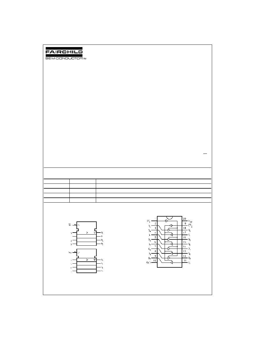
Ordering Code:
Devices also available in Tape and Reel. Specify by appending suffix letter "X" to the ordering code.
Logic Symbol
IEEE/IEC
Connection Diagram
Order Number
Package Number
Package Description
74LCX2244WM
M20B
20-Lead Small Outline Integrated Circuit (SOIC), JEDEC MS-013, 0.300" Wide
74LCX2244SJ
M20D
20-Lead Small Outline Package (SOP), EIAJ TYPE II, 5.3mm Wide
74LCX2244MSA
MSA20
20-Lead Shrink Small Outline Package (SSOP), EIAJ TYPE II, 5.3mm Wide
74LCX2244MTC
MTC20
20-Lead Thin Shrink Small Outline Package (TSSOP), JEDEC MO-153, 4.4mm Wide
3
www.fairchildsemi.com
7
4LCX2244
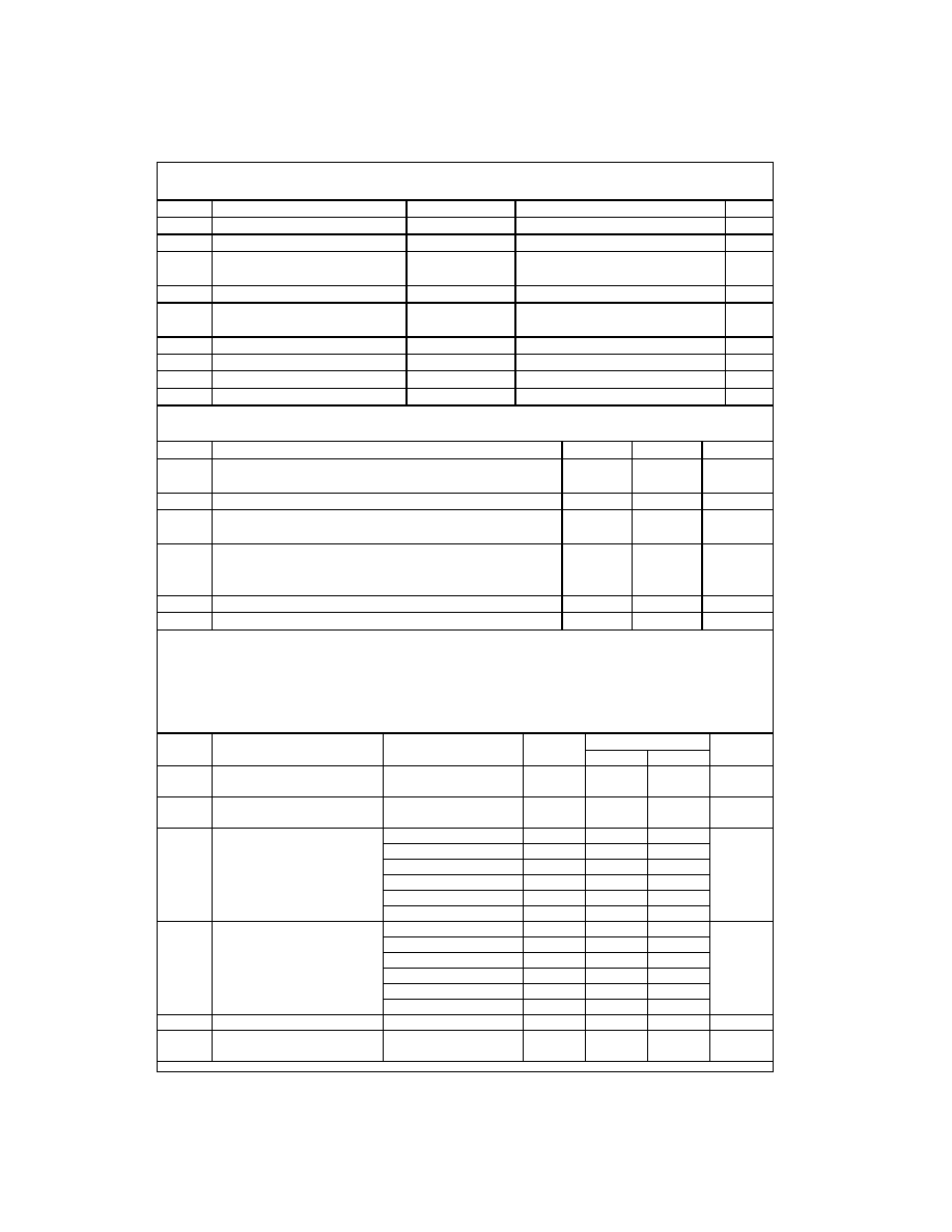
Absolute Maximum Ratings
(Note 2)
Recommended Operating Conditions
(Note 4)
Note 2: The Absolute Maximum Ratings are those values beyond which the safety of the device cannot be guaranteed. The device should not be operated
at these limits. The parametric values defined in the Electrical Characteristics tables are not guaranteed at the Absolute Maximum Ratings. The "Recom-
mended Operating Conditions" table will define the conditions for actual device operation.
Note 3: I
O
Absolute Maximum Rating must be observed.
Note 4: Unused inputs must be held HIGH or LOW. They may not float.
DC Electrical Characteristics
Symbol
Parameter
Value
Conditions
Units
V
CC
Supply Voltage
-
0.5 to
+
7.0
V
V
I
DC Input Voltage
-
0.5 to
+
7.0
V
V
O
DC Output Voltage
-
0.5 to
+
7.0
Output in 3-STATE
V
-
0.5 to V
CC
+
0.5
Output in HIGH or LOW State (Note 3)
I
IK
DC Input Diode Current
-
50
V
I
<
GND
mA
I
OK
DC Output Diode Current
-
50
V
O
<
GND
mA
+
50
V
O
>
V
CC
I
O
DC Output Source/Sink Current
±
50
mA
I
CC
DC Supply Current per Supply Pin
±
100
mA
I
GND
DC Ground Current per Ground Pin
±
100
mA
T
STG
Storage Temperature
-
65 to
+
150
∞
C
Symbol
Parameter
Min
Max
Units
V
CC
Supply Voltage
Operating
2.0
3.6
V
Data Retention
1.5
3.6
V
I
Input Voltage
0
5.5
V
V
O
Output Voltage
HIGH or LOW State
0
V
CC
V
3-STATE
0
5.5
I
OH
/I
OL
Output Current
V
CC
=
3.0V
-
3.6V
±
12
mA
V
CC
=
2.7V
-
3.0V
±
8
V
CC
=
2.3V
-
2.7V
±
4
T
A
Free-Air Operating Temperature
-
40
85
∞
C
t/
V
Input Edge Rate, V
IN
=
0.8V
-
2.0V, V
CC
=
3.0V
0
10
ns/V
Symbol
Parameter
Conditions
V
CC
T
A
=
-
40
∞
C to
+
85
∞
C
Units
(V)
Min
Max
V
IH
HIGH Level Input Voltage
2.3
-
2.7
1.7
V
2.7
-
3.6
2.0
V
IL
LOW Level Input Voltage
2.3
-
2.7
0.7
V
2.7
-
3.6
0.8
V
OH
HIGH Level Output Voltage
I
OH
=
-
100
µ
A
2.3
-
3.6
V
CC
-
0.2
V
I
OH
=
-
4 mA
2.3
1.8
I
OH
=
-
4 mA
2.7
2.2
I
OH
=
-
6 mA
3.0
2.4
I
OH
=
-
8mA
2.7
2.0
I
OH
=
-
12 mA
3.0
2.0
V
OL
LOW Level Output Voltage
I
OL
=
100
µ
A
2.3
-
3.6
0.2
V
I
OL
=
4 mA
2.3
0.6
I
OL
=
4 mA
2.7
0.4
I
OL
=
6 mA
3.0
0.55
I
OL
=
8 mA
2.7
0.6
I
OL
=
12 mA
3.0
0.8
I
I
Input Leakage Current
0
V
I
5.5V
2.3
-
3.6
±
5.0
µ
A
I
OZ
3-STATE Output Leakage
0
V
O
5.5V
2.3
-
3.6
±
5.0
µ
A
V
I
=
V
IH
or V
IL
www.fairchildsemi.com
4
74LCX2244
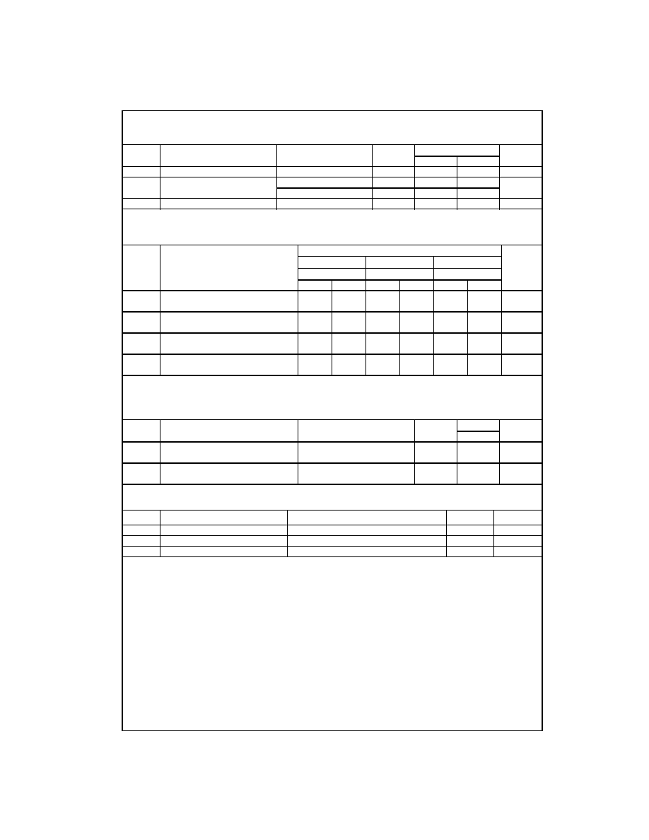
DC Electrical Characteristics
(Continued)
Note 5: Outputs disabled or 3-STATE only.
AC Electrical Characteristics
Note 6: Skew is defined as the absolute value of the difference between the actual propagation delay for any two separate outputs of the same device. The
specification applies to any outputs switching in the same direction, either HIGH-to-LOW (t
OSHL
) or LOW-to-HIGH (t
OSLH
).
Dynamic Switching Characteristics
Capacitance
Symbol
Parameter
Conditions
V
CC
T
A
=
-
40
∞
C to
+
85
∞
C
Units
(V)
Min
Max
I
OFF
Power-Off Leakage Current
V
I
or V
O
=
5.5V
0
10
µ
A
I
CC
Quiescent Supply Current
V
I
=
V
CC
or GND
2.3
-
3.6
10
µ
A
3.6V
V
I
, V
O
5.5V (Note 5)
2.3
-
3.6
±
10
I
CC
Increase in I
CC
per Input
V
IH
=
V
CC
-
0.6V
2.3
-
3.6
500
µ
A
Symbol
Parameter
T
A
=
-
40
∞
C to
+
85
∞
C, R
L
=
500
Units
V
CC
=
3.3V
±
0.3V
V
CC
=
2.7V
V
CC
=
2.5
±
0.2V
C
L
=
50pF
C
L
=
50pF
C
L
=
30pF
Min
Max
Min
Max
Min
Max
t
PHL
Propagation Delay
1.5
7.5
1.5
8.5
1.5
9.0
ns
t
PLH
Data to Output
1.5
7.5
1.5
8.5
1.5
9.0
t
PZL
Output Enable Time
1.5
9.0
1.5
10.0
1.5
10.5
ns
t
PZH
1.5
9.0
1.5
10.0
1.5
10.5
t
PLZ
Output Disable Time
1.5
7.0
1.5
8.0
1.5
8.4
ns
t
PHZ
1.5
7.0
1.5
8.0
1.5
8.4
t
OSHL
Output to Output Skew (Note 6)
1.0
ns
t
OSLH
1.0
Symbol
Parameter
Conditions
V
CC
(V)
T
A
=
25
∞
C
Units
Typical
V
OLP
Quiet Output Dynamic Peak V
OL
C
L
=
50 pF, V
IH
=
3.3V, V
IL
=
0V
3.3
0.35
V
C
L
=
30 pF, V
IH
=
2.5V, V
IL
=
0V
2.5
0.25
V
OLV
Quiet Output Dynamic Valley V
OL
C
L
=
50 pF, V
IH
=
3.3V, V
IL
=
0V
3.3
-
0.35
V
C
L
=
30 pF, V
IH
=
2.5V, V
IL
=
0V
2.5
-
0.25
Symbol
Parameter
Conditions
Typical
Units
C
IN
Input Capacitance
V
CC
=
Open, V
I
=
0V or V
CC
7
pF
C
OUT
Output Capacitance
V
CC
=
3.3V, V
I
=
0V or V
CC
8
pF
C
PD
Power Dissipation Capacitance
V
CC
=
3.3V, V
I
=
0V or V
CC
, f
=
10 MHz
25
pF
5
www.fairchildsemi.com
7
4LCX2244
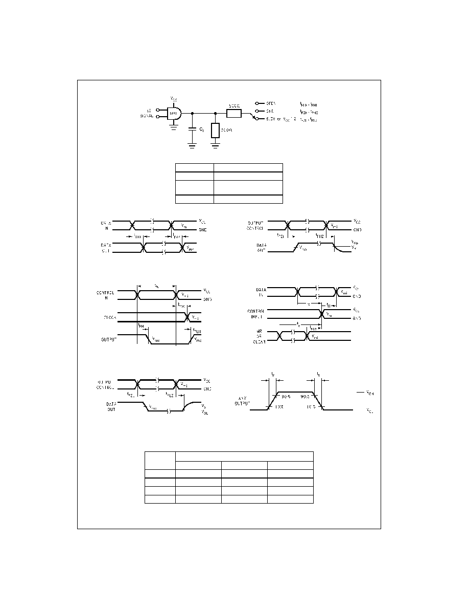
AC LOADING and WAVEFORMS
Generic for LCX Family
FIGURE 1. AC Test Circuit (C
L
includes probe and jig capacitance)
Waveform for Inverting and Non-Inverting Functions
Propagation Delay. Pulse Width and t
rec
Waveforms
3-STATE Output Low Enable and
Disable Times for Logic
3-STATE Output High Enable and
Disable Times for Logic
Setup Time, Hold Time and Recovery Time for Logic
t
rise
and t
fall
FIGURE 2. Waveforms
(Input Characteristics; f =1MHz, t
R
= t
F
= 3ns)
Test
Switch
t
PLH
, t
PHL
Open
t
PZL
, t
PLZ
6V at V
CC
=
3.3
±
0.3V
V
CC
x 2 at V
CC
=
2.5
±
0.2V
t
PZH
,t
PHZ
GND
Symbol
V
CC
3.3V
±
0.3V
2.7V
2.5V
±
0.2V
V
mi
1.5V
1.5V
V
CC
/2
V
mo
1.5V
1.5V
V
CC
/2
V
x
V
OL
+
0.3V
V
OL
+
0.3V
V
OL
+
0.15V
V
y
V
OH
-
0.3V
V
OH
-
0.3V
V
OH
-
0.15V