©2006 Fairchild Semiconductor Corporation
1
www.fairchildsemi.com
February 2006
74LCX573 Rev. 2.0.0
74LCX573 Lo
w
V
olta
g
e
Octal Latc
h with 5V
T
olerant Inputs and Outputs
74LCX573
Low Voltage Octal Latch with 5V Tolerant
Inputs and Outputs
Features
5V tolerant inputs and outputs
2.3V3.6V V
CC
specifications provided
7.0 ns t
PD
max (V
CC
= 3.3V), 10
µ
A I
CC
max
Power down high impedance inputs and outputs
Supports live insertion/withdrawal
1
±
24mA output drive (V
CC
= 3.0V)
Implements patented noise/EMI reduction circuitry
Latch-up performance exceeds JEDEC 78 conditions
ESD performance
Human body model
>
2000V
Machine model
>
200V
Leadless Pb-Free DQFN package
General Description
The LCX573 is a high-speed octal latch with buffered
common Latch Enable (LE) and buffered common Out-
put Enable (OE) input.
The LCX573 is functionally identical to the LCX373 but
has inputs and outputs on opposite sides.
The LCX573 is designed for low voltage applications with
capability of interfacing to a 5V signal environment. The
LCX573 is fabricated with an advanced CMOS tech-
nology to achieve high speed operation while maintain-
ing CMOS low power dissipation.
Ordering Information
Devices also available in Tape and Reel. Specify by appending the suffix letter "X" to the ordering code.
Pb-Free package per JEDEC J-STD-020B.
Notes
1.
To ensure the high impedance state during power up or down, OE should be tied to V
CC
through a pull-up resistor: the minimum
value of the resistor is determined by the current-sourcing capability of the driver.
2.
DQFN package available in Tape and Reel only.
3.
"_NL" indicates Pb-Free package (per JEDEC J-STD-020B). Device available in Tape and Reel only.
Order Number
Package
Number
Package Description
74LCX573WM
M20B
20-Lead Small Outline Integrated Circuit (SOIC), JEDEC MS-013, 0.300"
Wide
74LCX573SJ
M20D
20-Lead Small Outline Package (SOP), EIAJ TYPE II, 5.3mm Wide
74LCX573BQX
2
MLP020B
Pb-Free 20-Terminal Depopulated Quad Very-Thin Flat Pack No Leads
(DQFN), JEDEC MO-241, 2.5 x 4.5mm
74LCX573MSA
MSA20
20-Lead Shrink Small Outline Package (SSOP), JEDEC MO-150, 5.3mm
Wide
74LCX573MTC
MTC20
20-Lead Thin Shrink Small Outline Package (TSSOP), JEDEC MO-153,
4.4mm Wide
74LCX573MTCX_NL
3
MTC20
Pb-Free 20-Lead Thin Shrink Small Outline Package (TSSOP), JEDEC
MO-153, 4.4mm Wide
2
www.fairchildsemi.com
74LCX573 Rev. 2.0.0
74LCX573 Lo
w
V
olta
g
e
Octal Latc
h with 5V
T
olerant Inputs and Outputs
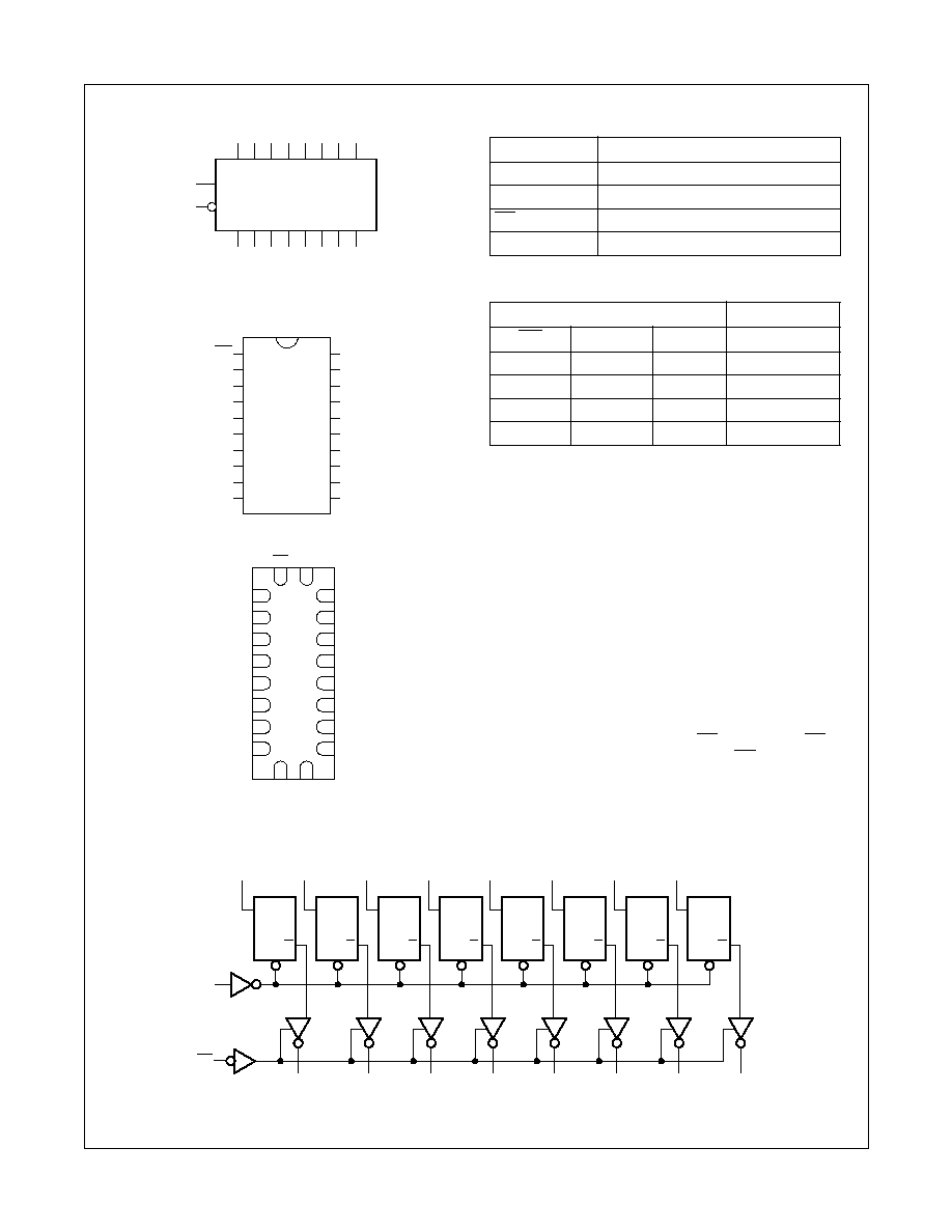
Logic Symbol
Connection Diagrams
Pin Assignments for
SOIC, SOP, SSOP, TSSOP
Pad Assignments for DQFN
(Top View)
Pin Descriptions
Truth Table
H = HIGH Voltage
L = LOW Voltage
Z = High Impedance
X = Immaterial
O
0
= Previous O
0
before HIGH-to-LOW transition of Latch
Enable
Functional Description
The LCX573 contains eight D-type latches with 3-STATE
output buffers. When the Latch Enable (LE) input is
HIGH, data on the D
n
inputs enters the latches. In this
condition the latches are transparent, i.e., a latch output
will change state each time its D input changes. When
LE is LOW the latches store the information that was
present on the D inputs a setup time preceding the
HIGH-to-LOW transition of LE. The 3-STATE buffers are
controlled by the Output Enable (OE) input. When OE is
LOW, the buffers are enabled. When OE is HIGH the
buffers are in the high impedance mode but this does not
interfere with entering new data into the latches.
D
0
D
1
D
2
D
3
D
4
D
5
D
6
D
7
O
0
OE
LE
O
1
O
2
O
3
O
4
O
5
O
6
O
7
D
1
D
2
D
3
D
4
D
5
D
6
D
7
GND
D
0
O
1
O
2
O
3
O
4
O
5
O
6
O
7
O
0
LE
V
CC
1
2
3
4
5
6
7
8
9
10
20
19
18
17
16
15
14
13
12
11
OE
D
1
D
2
D
3
D
4
D
5
D
6
D
7
GND
D
0
O
1
O
2
O
3
O
4
O
5
O
6
O
7
LE
O
0
V
CC
1
20
2
3
4
5
6
7
8
9
10
11
19
18
17
16
15
14
13
12
OE
Pin Names
Description
D
0
D
7
Data Inputs
LE
Latch Enable Input
OE
3-STATE Output Enable Input
O
0
O
7
3-STATE Latch Outputs
Inputs
Outputs
OE
LE
D
O
n
L
H
H
H
L
H
L
L
L
L
X
O
0
H
X
X
Z
Logic Diagram
Please note that this diagram is provided only for the understanding of logic operations and should not be used to estimate
propagation delays.
D
0
O
0
D
Q
LE
LE
OE
D
1
O
1
D
Q
LE
D
2
O
2
D
Q
LE
D
3
O
3
D
Q
LE
D
4
O
4
D
Q
LE
D
5
O
5
D
Q
LE
D
6
O
6
D
Q
LE
D
7
O
7
D
Q
LE
3
www.fairchildsemi.com
74LCX573 Rev. 2.0.0
74LCX573 Lo
w
V
olta
g
e
Octal Latc
h with 5V
T
olerant Inputs and Outputs
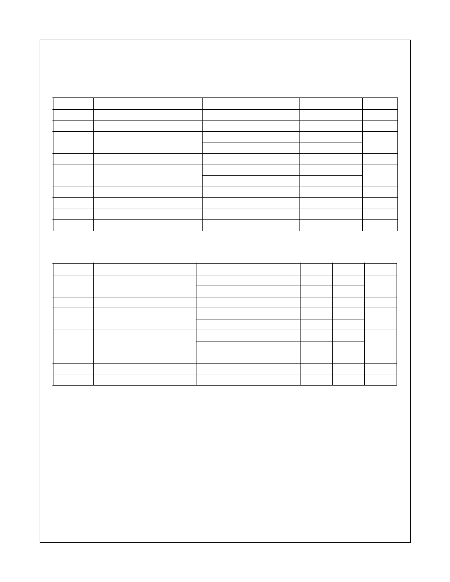
Absolute Maximum Ratings
The Absolute Maximum Ratings are those values beyond which the safety of the device cannot be guaranteed. The
device should not be operated at these limits. The parametric values defined in the Electrical Characteristics tables are
not guaranteed at the Absolute Maximum Ratings. The "Recommended Operating Conditions" table will define the
conditions for actual device operation.
Recommended Operating Conditions
5
Notes:
4.
I
O
Absolute Maximum Rating must be observed.
5.
Unused (inputs or I/Os) must be held HIGH or LOW. They may not float.
Symbol
Parameter
Conditions
Value
Units
V
CC
Supply Voltage
-
0.5 to
+
7.0
V
V
I
DC Input Voltage
-
0.5 to
+
7.0
V
V
O
DC Output Voltage
Output in 3-STATE
-
0.5 to
+
7.0
V
Output in HIGH or LOW State
4
-
0.5 to V
CC
+
0.5
I
IK
DC Input Diode Current
V
I
<
GND
-
50
mA
I
OK
DC Output Diode Current
V
O
<
GND
-
50
mA
V
O
>
V
CC
+
50
I
O
DC Output Source/Sink Current
±
50
mA
I
CC
DC Supply Current per Supply Pin
±
100
mA
I
GND
DC Ground Current per Ground Pin
±
100
mA
T
STG
Storage Temperature
-
65 to
+
150
°
C
Symbol
Parameter
Conditions
Min.
Max.
Units
V
CC
Supply Voltage
Operating
2.0
3.6
V
Data Retention
1.5
3.6
V
I
Input Voltage
0
5.5
V
V
O
Output Voltage
HIGH or LOW State
0
V
CC
V
3-STATE
0
5.5
I
OH
/
I
OL
Output Current
V
CC
= 3.0V
-
3.6V
±
24
mA
V
CC
= 2.7V
-
3.0V
±
12
V
CC
= 2.3V
-
2.7V
±
8
T
A
Free-Air Operating Temperature
-
40
85
°
C
t
/
V
Input Edge Rate
V
IN
= 0.8V
-
2.0V, V
CC
= 3.0V
0
10
ns
/
V
4
www.fairchildsemi.com
74LCX573 Rev. 2.0.0
74LCX573 Lo
w
V
olta
g
e
Octal Latc
h with 5V
T
olerant Inputs and Outputs
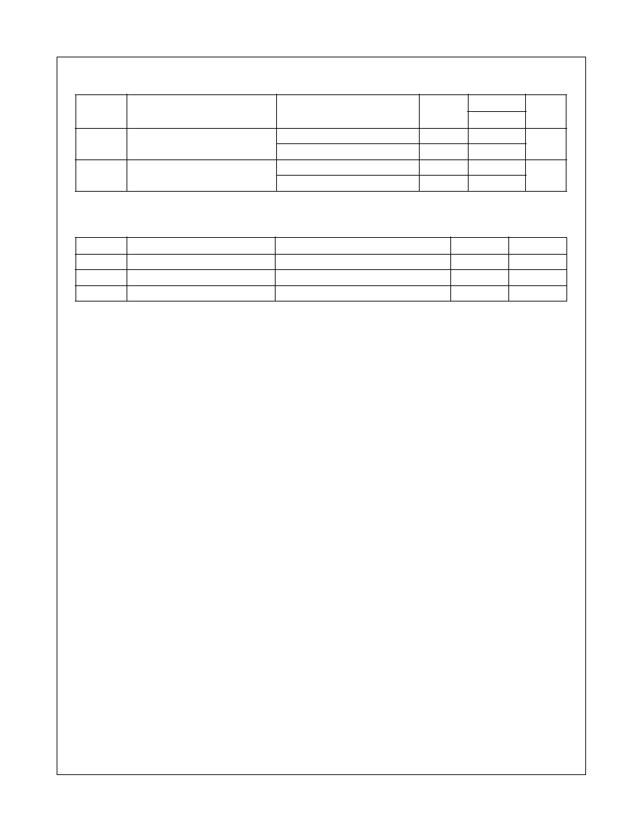
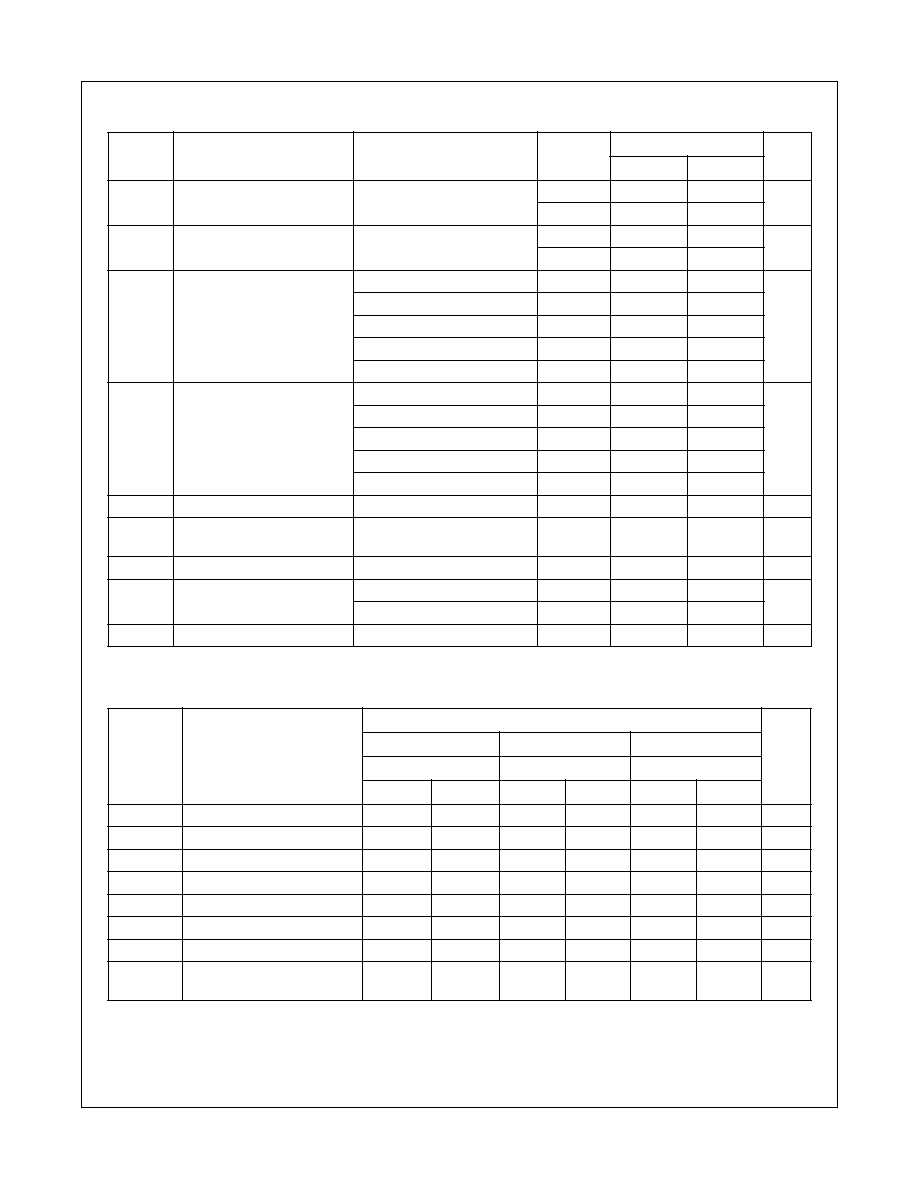
DC Electrical Characteristics
AC Electrical Characteristics
Notes:
6.
Outputs disabled or 3-STATE only.
7.
Skew is defined as the absolute value of the difference between the actual propagation delay for any two separate outputs of the
same device. The specification applies to any outputs switching in the same direction, either HIGH-to-LOW (t
OSHL
) or LOW-to-
HIGH (t
OSLH
).
Symbol
Parameter
Conditions
V
CC
(V)
T
A
=
-
40
°
C to
+
85
°
C
Units
Min.
Max.
V
IH
HIGH Level Input Voltage
2.3
-
2.7
1.7
V
2.7
-
3.6
2.0
V
IL
LOW Level Input Voltage
2.3
-
2.7
0.7
V
2.7
-
3.6
0.8
V
OH
HIGH Level Output
Voltage
I
OH
=
-
100
µ
A
2.3
-
3.6
V
CC
-
0.2
V
I
OH
=
-
8mA
2.3
1.8
I
OH
=
-
12mA
2.7
2.2
I
OH
=
-
18mA
3.0
2.4
I
OH
=
-
24mA
3.0
2.2
V
OL
LOW Level Output
Voltage
I
OL
= 100
µ
A
2.3
-
3.6
0.2
V
I
OL
= 8mA
2.3
0.6
I
OL
= 12mA
2.7
0.4
I
OL
= 16mA
3.0
0.4
I
OL
= 24mA
3.0
0.55
I
I
Input Leakage Current
0
V
I
5.5V
2.3
-
3.6
±
5.0
µ
A
I
OZ
3-STATE Output Leakage
0
V
O
5.5V, V
I
= V
IH
or
V
IL
2.3
-
3.6
±
5.0
µ
A
I
OFF
Power-Off Leakage Current
V
I
or V
O
= 5.5V
0
10
µ
A
I
CC
Quiescent Supply Current
V
I
= V
CC
or GND
2.3
-
3.6
10
µ
A
3.6V
V
I
, V
O
5.5V
6
2.3
-
3.6
±
10
I
CC
Increase in I
CC
per Input
V
IH
= V
CC
-
0.6V
2.3
-
3.6
500
µ
A
Symbol
Parameter
T
A
=
-
40
°
C to
+
85
°
C, R
L
= 500
Units
V
CC
= 3.3V
±
0.3V
V
CC
= 2.7V
V
CC
= 2.5
±
0.2V
C
L
= 50pF
C
L
= 50pF
C
L
= 30pF
Min.
Max.
Min.
Max.
Min.
Max.
t
PHL
, t
PLH
Propagation Delay, D
n
to O
n
1.5
8.0
1.5
9.0
1.5
9.6
ns
t
PHL
, t
PLH
Propagation Delay, LE to O
n
1.5
8.5
1.5
9.5
1.5
10.5
ns
t
PZL
, t
PZH
Output Enable Time
1.5
8.5
1.5
9.5
1.5
10.5
ns
t
PLZ
, t
PHZ
Output Disable Time
1.5
6.5
1.5
7.0
1.5
7.8
ns
t
S
Setup Time, D
n
to LE
2.5
2.5
4.0
ns
t
H
Hold Time, D
n
to LE
1.5
1.5
2.0
ns
t
W
LE Pulse Width
3.3
3.3
4.0
ns
t
OSHL
,
t
OSLH
Output to Output Skew
7
1.0
ns