© 2003 Fairchild Semiconductor Corporation
DS500727
www.fairchildsemi.com
April 2002
Revised August 2003
7
4
LCXH
3
2245 Lo
w
V
o
lt
age 3
2
-Bi
t
Bidi
rect
iona
l
T
r
ansce
iver
wi
th
5V T
o
l
e
rant
I
nput
s and
Output
s
w
i
th
Bushol
d
74LCXH32245
Low Voltage 32-Bit Bidirectional Transceiver
with 5V Tolerant Inputs and Outputs with Bushold
General Description
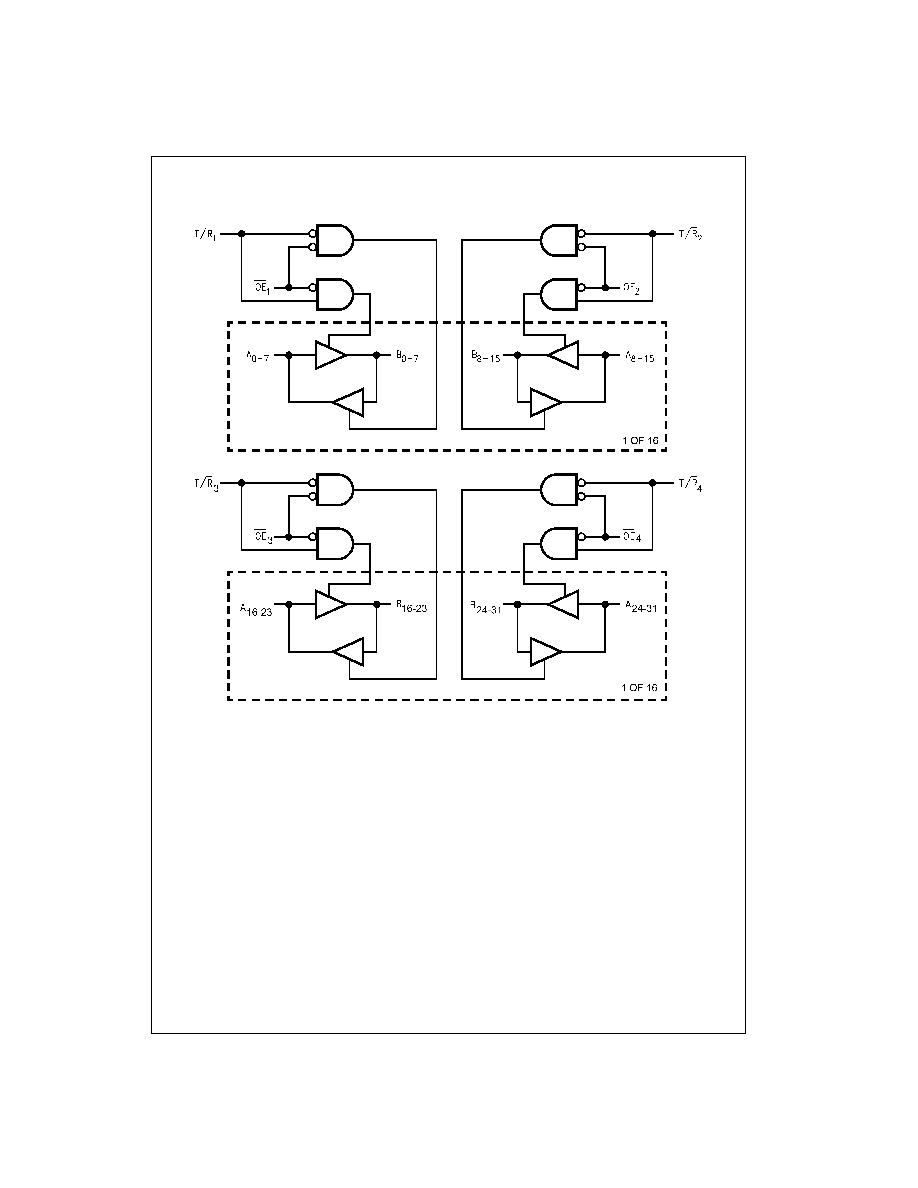
The LCXH32245 contains thirty-two non-inverting bidirec-
tional buffers with 3-STATE outputs and is intended for bus
oriented applications. The device is designed for low volt-
age (2.5V or 3.3V) V
CC
applications with capability of inter-
facing to a 5V signal environment. The device is byte
controlled. Each byte has separate control inputs which
could be shorted together for full 32-bit operation. The T/R
inputs determine the direction of data flow through the
device. The OE inputs disable both the A and B ports by
placing them in a high impedance state.
The LCXH32245 data inputs include bushold, eliminating
the need for external pull-up/down resistors to hold unused
inputs.
The LCXH32245 is fabricated with an advanced CMOS
technology to achieve high speed operation while maintain-
ing CMOS low power dissipation.
Features
s
5V tolerant inputs and outputs
s
2.3V to 3.6V V
CC
specifications provided
s
4.5 ns t
PD
max (V
CC
=
3.3V), 20
µ
A I
CC
max
s
Power-off high impedance inputs and outputs
s
Bushold on inputs eliminates the need for external
pull-up/down resistors
s
Supports live insertion/withdrawal (Note 1)
s
±
24 mA output drive (V
CC
=
3.0V)
s
Uses patented noise/EMI reduction circuitry
s
Latch-up performance exceeds 500 mA
s
ESD performance:
Human body model
>
2000V
Machine model
>
200V
s
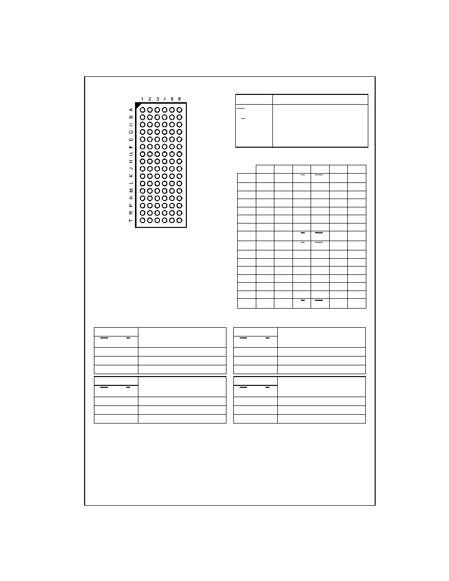
Packaged in plastic Fine-Pitch Ball Grid Array (FBGA)
Note 1: To ensure the high-impedance state during power-up or down, OE
should be tied to VCC through a pull-up resistor: the minimum value or the
resistor is determined by the current-sourcing capability of the driver.
Ordering Code:
Note 2: Ordering Code "G" indicates Trays.
Note 3: Devices also available in Tape and Reel. Specify by appending the suffix letter "X" to the ordering code.
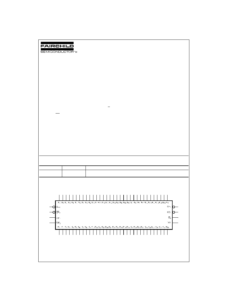
Logic Symbol
Order Number
Package Number
Package Description
74LCXH32245G
(Note 2) (Note 3)
BGA96A
96-Ball Fine-Pitch Ball Grid Array (FBGA), JEDEC MO-205, 5.5mm Wide

www.fairchildsemi.com
4
74LCXH32245
Absolute Maximum Ratings
(Note 4)
Recommended Operating Conditions
(Note 6)
Note 4: The Absolute Maximum Ratings are those values beyond which the safety of the device cannot be guaranteed. The device should not be operated
at these limits. The parametric values defined in the Electrical Characteristics tables are not guaranteed at the Absolute Maximum Ratings. The "Recom-
mended Operating Conditions" table will define the conditions for actual device operation.
Note 5: I
O
Absolute Maximum Rating must be observed.
Note 6: Floating or unused control inputs must be HIGH or LOW.
DC Electrical Characteristics
Symbol
Parameter
Value
Conditions
Units
V
CC
Supply Voltage
-
0.5 to
+
7.0
V
V
I
T/R, OE
-
0.5 to
+
7.0
V
I/O Ports
-
0.5 to V
CC
+
0.5
V
O
DC Output Voltage
-
0.5 to
+
7.0
Output in 3-STATE
V
-
0.5 to V
CC
+
0.5
Output in HIGH or LOW State (Note 5)
I
IK
DC Input Diode Current
-
50
V
I
<
GND
mA
I
OK
DC Output Diode Current
-
50
V
O
<
GND
mA
+
50
V
O
>
V
CC
I
O
DC Output Source/Sink Current
±
50
mA
I
CC
DC Supply Current per Supply Pin
±
100
mA
I
GND
DC Ground Current per Ground Pin
±
100
mA
T
STG
Storage Temperature
-
65 to
+
150
∞
C
Symbol
Parameter
Min
Max
Units
V
CC
Supply Voltage
Operating
2.0
3.6
V
Data Retention
1.5
3.6
V
I
Input Voltage
0
V
CC
V
V
O
Output Voltage
HIGH or LOW State
0
V
CC
V
3-STATE
0
5.5
I
OH
/I
OL
Output Current
V
CC
=
3.0V
-
3.6V
±
24
mA
V
CC
=
2.7V
-
3.0V
±
12
V
CC
=
2.3V
-
2.7V
±
8
T
A
Free-Air Operating Temperature
-
40
85
∞
C
t/
V
Input Edge Rate, V
IN
=
0.8V≠2.0V, V
CC
=
3.0V
0
10
ns/V
Symbol
Parameter
Conditions
V
CC
T
A
=
-
40
∞
C to
+
85
∞
C
Units
(V)
Min
Max
V
IH
HIGH Level Input Voltage
2.3
-
2.7
1.7
V
2.7
-
3.6
2.0
V
IL
LOW Level Input Voltage
2.3
-
2.7
0.7
V
2.7
-
3.6
0.8
V
OH
HIGH Level Output Voltage
I
OH
=
-
100
µ
A
2.3
-
3.6
V
CC
-
0.2
V
I
OH
=
-
8 mA
2.3
1.8
I
OH
=
-
12 mA
2.7
2.2
I
OH
=
-
18 mA
3.0
2.4
I
OH
=
-
24 mA
3.0
2.2
V
OL
LOW Level Output Voltage
I
OL
=
100
µ
A
2.3
-
3.6
0.2
V
I
OL
=
8 mA
2.3
0.6
I
OL
=
12 mA
2.7
0.4
I
OL
=
16 mA
3.0
0.4
I
OL
=
24 mA
3.0
0.55

5
www.fairchildsemi.com
7
4
LCXH
3
2245
DC Electrical Characteristics
(Continued)
Note 7: An external driver must source at least the specified current to switch from LOW-to-HIGH.
Note 8: An external driver must sink at least the specified current to switch from HIGH-to-LOW.
Note 9: Outputs disabled or 3-STATE only.
AC Electrical Characteristics
Dynamic Switching Characteristics
Capacitance
Symbol
Parameter
Conditions
V
CC
T
A
=
-
40
∞
C to
+
85
∞
C
Units
(V)
Min
Max
I
I
Input Leakage Current
0
V
I
5.5V
2.3
-
3.6
±
5.0
µ
A
I
I(HOLD)
Bushold Input Minimum
V
IN
=
0.7V
2.3
45
Drive Hold Current
V
IN
=
1.7V
-45
V
IN
=
0.8V
3.0
75
V
IN
=
2.0V
-
75
I
I(OD)
Bushold Input Over-Drive
(Note 7)
2.7
300
µ
A
Current to Change State
(Note 8)
-
300
(Note 7)
3.6
450
(Note 8)
-
450
I
OZ
3-STATE I/O Leakage
0
V
O
5.5V
2.3
-
3.6
±
5.0
µ
A
V
I
=
V
IH
or V
IL
I
OFF
Power-Off Leakage Current
V
I
or V
O
=
5.5V
0
10
µ
A
I
CC
Quiescent Supply Current
V
I
=
V
CC
or GND
2.3≠3.6
20
µ
A
3.6V
V
I
, V
O
5.5V (Note 9)
2.3≠3.6
±
20
I
CC
Increase in I
CC
per Input
V
IH
=
V
CC
-
0.6V
2.3≠3.6
500
µ
A
Symbol
Parameter
T
A
=
-
40
∞
C to
+
85
∞
C, R
L
=
500
Units
V
CC
=
3.3V
±
0.3V
V
CC
=
2.7V
V
CC
=
2.5V
±
0.2V
C
L
=
50 pF
C
L
=
50 pF
C
L
=
30 pF
Min
Max
Min
Max
Min
Max
t
PHL
Propagation Delay
1.0
4.5
1.0
5.2
1.0
5.4
ns
t
PLH
A
n
to B
n
or B
n
to A
n
1.0
4.5
1.0
5.2
1.0
5.4
t
PZL
Output Enable Time
1.0
6.5
1.0
7.2
1.0
8.5
ns
t
PZH
1.0
6.5
1.0
7.2
1.0
8.5
t
PLZ
Output Disable Time
1.0
6.4
1.0
6.9
1.0
7.7
ns
t
PHZ
1.0
6.4
1.0
6.9
1.0
7.7
Symbol
Parameter
Conditions
V
CC
T
A
=
25
∞
C
Units
(V)
Typical
V
OLP
Quiet Output Dynamic Peak V
OL
C
L
=
50 pF, V
IH
=
3.3V, V
IL
=
0V
3.3
0.8
V
C
L
=
30 pF, V
IH
=
2.5V, V
IL
=
0V
2.5
0.6
V
OLV
Quiet Output Dynamic Valley V
OL
C
L
=
50 pF, V
IH
=
3.3V, V
IL
=
0V
3.3
-
0.8
V
C
L
=
30 pF, V
IH
=
2.5V, V
IL
=
0V
2.5
-
0.6
Symbol
Parameter
Conditions
Typical
Units
C
IN
Input Capacitance
V
CC
=
Open, V
I
=
0V or V
CC
7
pF
C
I/O
Input/Output Capacitance
V
CC
=
3.3V, V
I
=
0V or V
CC
8
pF
C
PD
Power Dissipation Capacitance
V
CC
=
3.3V, V
I
=
0V or V
CC
, f
=
10 MHz
20
pF