Preliminary
© 2000 Fairchild Semiconductor Corporation
DS500257
www.fairchildsemi.com
February 2000
Revised February 2000
7
4LCXZ16240 Low
V
o
lt
age 16-Bi
t Inv
e
rt
ing Buff
er/
L
ine
Dri
ver wit
h
5
V
T
o
le
rant
I
nputs/
Output
s (Pre
li
m
i
nary)
74LCXZ16240
Low Voltage 16-Bit Inverting Buffer/Line Driver with
5V Tolerant Inputs/Outputs (Preliminary)
General Description
The LCXZ16240 contains sixteen inverting buffers with 3-
STATE outputs designed to be employed as a memory and
address driver, clock driver, or bus-oriented transmitter/
receiver. The device is nibble controlled. Each nibble has
separate 3-STATE control inputs which can be shorted
together for full 16-bit operation.
When V
CC
is between 0 and 1.5V, the LCXZ16240 is in the
high impedance state during power up or power down. This
places the outputs in the high impedance (Z) state prevent-
ing intermittent low impedance loading or glitching in bus
oriented applications.
The LCXZ16240 is designed for low voltage (2.7V or 3.3V)
V
CC
applications with capacity of interfacing to a 5V signal
environment.
The LCXZ16240 is fabricated with an advanced CMOS
technology to achieve high speed operation while maintain-
ing CMOS low power dissipation.
Features
s
5V tolerant inputs and outputs
s
Guaranteed power up/down high impedance
s
Supports live insertion/withdrawal
s
2.7V≠3.6V V
CC
specifications provided
s
4.5 ns t
PD
max (V
CC
=
3.3V), 20
µ
A I
CC
max
s
±
24 mA output drive (V
CC
=
3.0V)
s
Implements patented noise/EMI reduction circuitry
s
Latch-up performance exceeds 500 mA
s
ESD performance:
Human body model
>
2000V
Machine model
>
200V
Ordering Code:
Devices also available in Tape and Reel. Specify by appending the suffix letter "X" to the ordering code.
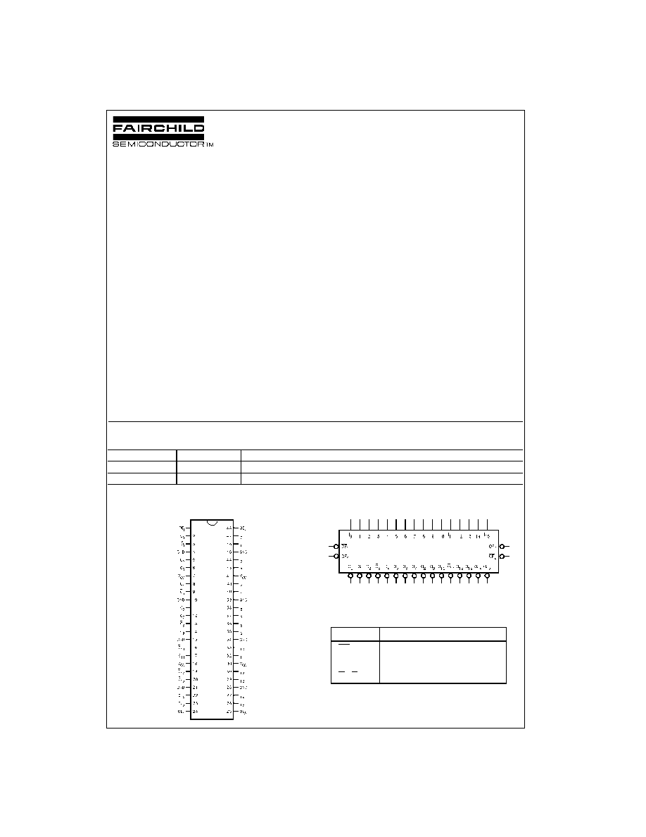
Connection Diagram
Logic Symbol
Pin Descriptions
Order Number
Package Number
Package Description
74LCXZ16240MEA
MS48A
48-Lead Small Shrink Outline Package (SSOP), JEDEC MO-118, 0.300" Wide
74LCXZ16240MTD
MTD48
48-Lead Thin Shrink Small Outline Package (TSSOP), JEDEC MO-153, 6.1mm Wide
Pin Names
Description
OE
n
Output Enable Inputs (Active LOW)
I
0
≠I
15
Inputs
O
0
≠O
15
Outputs
Preliminary
www.fairchildsemi.com
2
74LCXZ16240
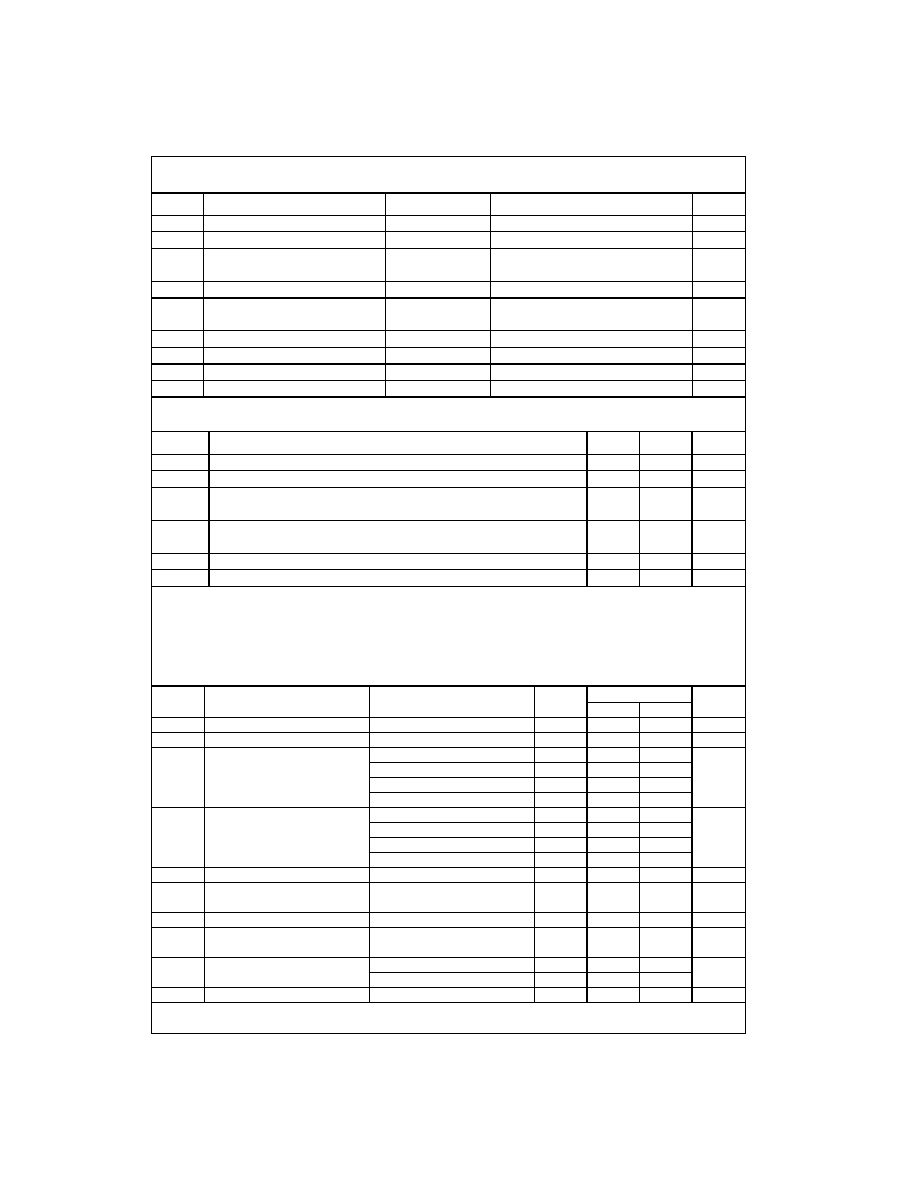
Truth Tables
H
=
HIGH Voltage Level
L
=
LOW Voltage Level
X
=
Immaterial
Z
=
High Impedance
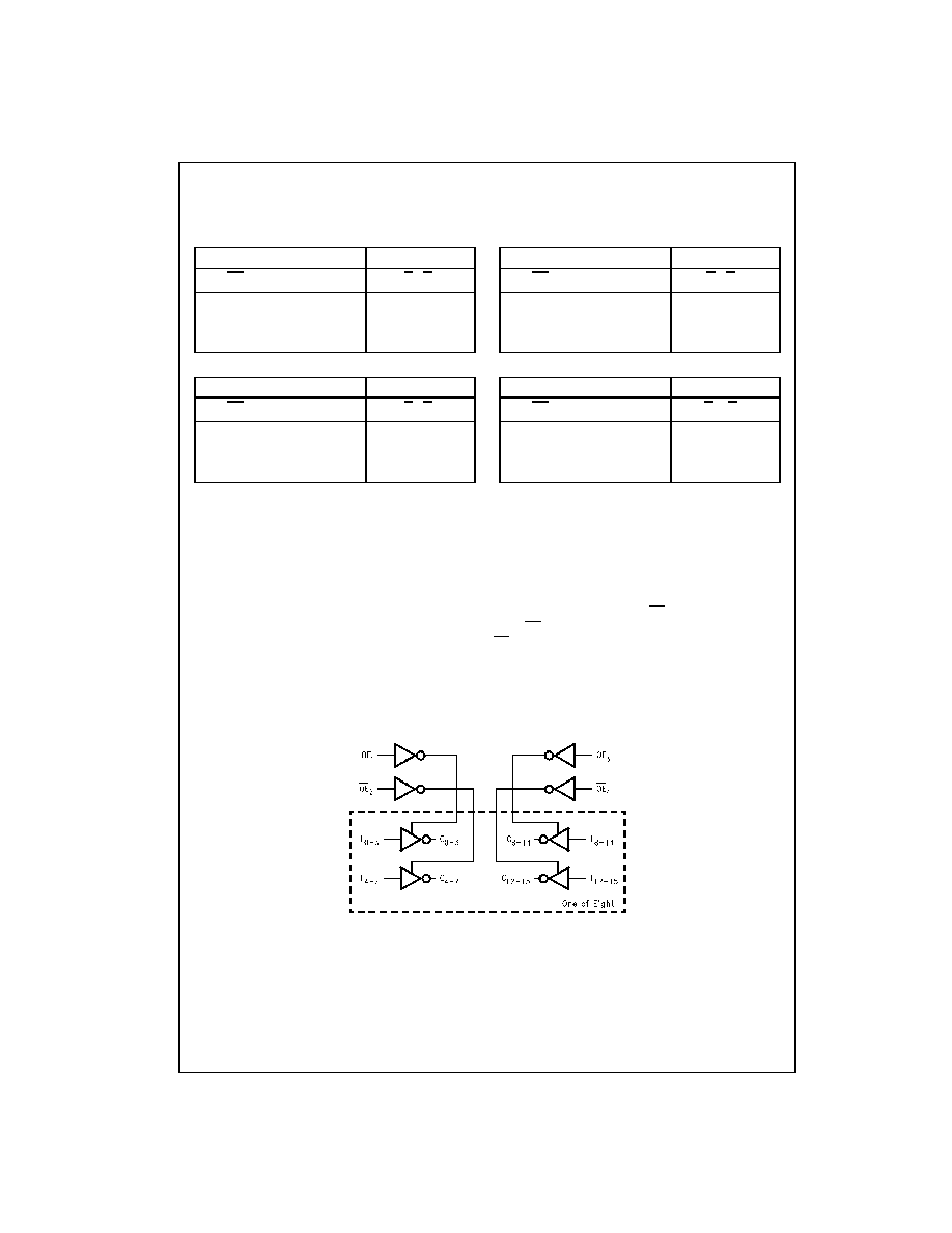
Functional Description
The LCXZ16240 contains sixteen inverting buffers with 3-
STATE standard outputs. The device is nibble (4 bits) con-
trolled with each nibble functioning identically, but indepen-
dent of the other. The control pins may be shorted together
to obtain full 16-bit operation. The 3-STATE outputs are
controlled by an Output Enable (OE
n
) input for each nibble.
When OE
n
is LOW, the outputs are in 2-state mode. When
OE
n
is HIGH, the outputs are in the high impedance mode,
but this does not interfere with entering new data into the
inputs.
Logic Diagram
Inputs
Outputs
OE
1
I
0
≠I
3
O
0
≠O
3
L
L
H
L
H
L
H
X
Z
Inputs
Outputs
OE
3
I
8
≠I
11
O
8
≠O
11
L
L
H
L
H
L
H
X
Z
Inputs
Outputs
OE
2
I
4
≠I
7
O
4
≠O
7
L
L
H
L
H
L
H
X
Z
Inputs
Outputs
OE
4
I
12
≠I
15
O
12
≠O
15
L
L
H
L
H
L
H
X
Z
Preliminary
3
www.fairchildsemi.com
7
4LCXZ16240
Absolute Maximum Ratings
(Note 1)
Recommended Operating Conditions
(Note 3)
Note 1: The Absolute Maximum Ratings are those values beyond which the safety of the device cannot be guaranteed. The device should not be operated
at these limits. The parametric values defined in the Electrical Characteristics tables are not guaranteed at the Absolute Maximum Ratings. The "Recom-
mended Operating Conditions" table will define the conditions for actual device operation.
Note 2: I
O
Absolute Maximum Rating must be observed.
Note 3: Unused inputs must be held HIGH or LOW. They may not float.
DC Electrical Characteristics
Note 4: Outputs disabled or 3-STATE only.
Symbol
Parameter
Value
Conditions
Units
V
CC
Supply Voltage
-
0.5 to
+
7.0
V
V
I
DC Input Voltage
-
0.5 to
+
7.0
V
V
O
DC Output Voltage
-
0.5 to
+
7.0
Output in 3-STATE or V
CC
=
0≠1.5V
V
-
0.5 to V
CC
+
0.5
Output in HIGH or LOW State (Note 2)
I
IK
DC Input Diode Current
-
50
V
I
<
GND
mA
I
OK
DC Output Diode Current
-
50
V
O
<
GND
mA
+
50
V
O
>
V
CC
I
O
DC Output Source/Sink Current
±
50
mA
I
CC
DC Supply Current per Supply Pin
±
100
mA
I
GND
DC Ground Current per Ground Pin
±
100
mA
T
STG
Storage Temperature
-
65 to
+
150
∞
C
Symbol
Parameter
Min
Max
Units
V
CC
Supply Voltage
Operating
2.7
3.6
V
V
I
Input Voltage
0
5.5
V
V
O
Output Voltage
HIGH or LOW State
0
V
CC
V
3-STATE or V
CC
=
OFF
0
5.5
I
OH
/I
OL
Output Current
V
CC
=
3.0V
-
3.6V
±
24
mA
V
CC
=
2.7V
-
3.0V
±
12
T
A
Free-Air Operating Temperature
-
40
85
∞
C
t/
V
Input Edge Rate, V
IN
=
0.8V≠2.0V, V
CC
=
3.0V
0
10
ns/V
Symbol
Parameter
Conditions
V
CC
T
A
=
-
40
∞
C to
+
85
∞
C
Units
(V)
Min
Max
V
IH
HIGH Level Input Voltage
2.7
-
3.6
2.0
V
V
IL
LOW Level Input Voltage
2.7
-
3.6
0.8
V
V
OH
HIGH Level Output Voltage
I
OH
=
-
100
µ
A
2.7
-
3.6
V
CC
-
0.2
V
I
OH
=
-
12 mA
2.7
2.2
I
OH
=
-
18 mA
3.0
2.4
I
OH
=
-
24 mA
3.0
2.2
V
OL
LOW Level Output Voltage
I
OL
=
100
µ
A
2.7
-
3.6
0.2
V
I
OL
=
12 mA
2.7
0.4
I
OL
=
16 mA
3.0
0.4
I
OL
=
24 mA
3.0
0.55
I
I
Input Leakage Current
0
V
I
5.5V
2.7
-
3.6
±
5.0
µ
A
I
OZ
3-STATE Output Leakage
0
V
O
5.5V
2.7
-
3.6
±
5.0
µ
A
V
I
=
V
IH
or V
IL
I
OFF
Power-Off Leakage Current
V
I
or V
O
=
5.5V
0
10
µ
A
I
PU/PD
Power Up/Down
V
O
=
0.5V to V
CC
0
-
1.5
±
5.0
µ
A
3-STATE Output Current
V
I
=
GND or V
CC
I
CC
Quiescent Supply Current
V
I
=
V
CC
or GND
2.7
-
3.6
225
µ
A
3.6V
V
I
, V
O
5.5V (Note 4)
2.7
-
3.6
±
225
I
CC
Increase in I
CC
per Input
V
IH
=
V
CC
-
0.6V
2.7
-
3.6
500
µ
A

Preliminary
www.fairchildsemi.com
4
74LCXZ16240
AC Electrical Characteristics
Note 5: Skew is defined as the absolute value of the difference between the actual propagation delay for any two separate outputs of the same device. The
specification applies to any outputs switching in the same direction, either HIGH-to-LOW (t
OSHL
) or LOW-to-HIGH (t
OSLH
).
Dynamic Switching Characteristics
Capacitance
Symbol
Parameter
T
A
=
-
40
∞
C to
+
85
∞
C, R
L
=
500
Units
V
CC
=
3.3V
±
0.3V
V
CC
=
2.7V
C
L
=
50 pF
C
L
=
50 pF
Min
Max
Min
Max
t
PHL
Propagation Delay
1.5
4.5
1.5
5.3
ns
t
PLH
Data to Output
1.5
4.5
1.5
5.3
t
PZL
Output Enable Time
1.5
5.4
1.5
6.0
ns
t
PZH
1.5
5.4
1.5
6.0
t
PLZ
Output Disable Time
1.5
5.3
1.5
5.4
ns
t
PHZ
1.5
5.3
1.5
5.4
t
OSHL
Output to Output Skew (Note 5)
1.0
ns
t
OSLH
1.0
Symbol
Parameter
Conditions
V
CC
(V)
T
A
=
25
∞
C
Unit
Typical
V
OLP
Quiet Output Dynamic Peak V
OL
C
L
=
50 pF, V
IH
=
3.3V, V
IL
=
0V
3.3
0.8
V
V
OLV
Quiet Output Dynamic Valley V
OL
C
L
=
50 pF, V
IH
=
3.3V, V
IL
=
0V
3.3
-
0.8
V
Symbol
Parameter
Conditions
Typical
Units
C
IN
Input Capacitance
V
CC
=
Open, V
I
=
0V or V
CC
7
pF
C
OUT
Output Capacitance
V
CC
=
3.3V, V
I
=
0V or V
CC
8
pF
C
PD
Power Dissipation Capacitance
V
CC
=
3.3V, V
I
=
0V or V
CC
, f
=
10 MHz
20
pF

Preliminary
5
www.fairchildsemi.com
7
4LCXZ16240
AC LOADING and WAVEFORMS
Generic for LCX Family
FIGURE 1. AC Test Circuit (C
L
includes probe and jig capacitance)
Waveform for Inverting and Non-Inverting Functions
Propagation Delay. Pulse Width and t
rec
Waveforms
3-STATE Output Low Enable and
Disable Times for Logic
3-STATE Output High Enable and
Disable Times for Logic
Setup Time, Hold Time and Recovery Time for Logic
t
rise
and t
fall
FIGURE 2. Waveforms
(Input Characteristics; f =1MHz, t
R
= t
F
= 3ns)
V
I
C
L
6V for V
CC
=
3.3V, 2.7V
50 pF
V
CC
* 2 for V
CC
=
2.5V
30 pF
Symbol
V
CC
3.3V
±
0.3V
2.7V
V
mi
1.5V
1.5V
V
mo
1.5V
1.5V
V
x
V
OL
+
0.3V
V
OL
+
0.3V
V
y
V
OH
-
0.3V
V
OH
-
0.3V