 | –≠–ª–µ–∫—Ç—Ä–æ–Ω–Ω—ã–π –∫–æ–º–ø–æ–Ω–µ–Ω—Ç: 74LS164 | –°–∫–∞—á–∞—Ç—å:  PDF PDF  ZIP ZIP |
© 2000 Fairchild Semiconductor Corporation
DS006398
www.fairchildsemi.com
August 1986
Revised April 2000
DM74LS164
8-
Bit
Ser
i
al
I
n
/Pa
r
al
lel
Out
Shi
f
t
Regi
ste
r
DM74LS164
8-Bit Serial In/Parallel Out Shift Register
General Description
These 8-bit shift registers feature gated serial inputs and
an asynchronous clear. A low logic level at either input
inhibits entry of the new data, and resets the first flip-flop to
the low level at the next clock pulse, thus providing com-
plete control over incoming data. A high logic level on
either input enables the other input, which will then deter-
mine the state of the first flip-flop. Data at the serial inputs
may be changed while the clock is HIGH or LOW, but only
information meeting the setup and hold time requirements
will be entered. Clocking occurs on the LOW-to-HIGH level
transition of the clock input. All inputs are diode-clamped to
minimize transmission-line effects.
Features
s
Gated (enable/disable) serial inputs
s
Fully buffered clock and serial inputs
s
Asynchronous clear
s
Typical clock frequency 36 MHz
s
Typical power dissipation 80 mW
Ordering Code:
Devices also available in Tape and Reel. Specify by appending the suffix letter "X" to the ordering code.
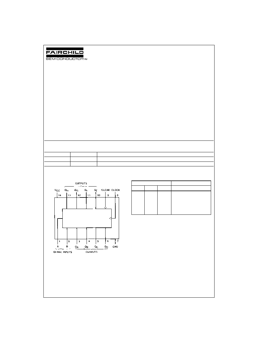
Connection Diagram
Function Table
H
=
HIGH Level (steady state)
L
=
LOW Level (steady state)
X
=
Don't Care (any input, including transitions)
=
Transition from LOW-to-HIGH level
Q
A0
, Q
B0
, Q
H0
=
The level of Q
A
, Q
B
, or Q
H
, respectively, before the
indicated steady-state input conditions were established.
Q
An
, Q
Gn
=
The level of Q
A
or Q
G
before the most recent
transition of the
clock; indicates a one-bit shift.
Order Number
Package Number
Package Description
DM74LS164M
M14A
14-Lead Small Outline Integrated Circuit (SOIC), JEDEC MS-120, 0.150 Narrow
DM74LS164N
N14A
14-Lead Plastic Dual-In-Line Package (PDIP), JEDEC MS-001, 0.300 Wide
Inputs
Outputs
Clear
Clock
A
B
Q
A
Q
B
...
Q
H
L
X
X
X
L
L
...
L
H
L
X
X
Q
A0
Q
B0
...
Q
H0
H
H
H
H
Q
An
...
Q
Gn
H
L
X
L
Q
An
...
Q
Gn
H
X
L
L
Q
An
...
Q
Gn

www.fairchildsemi.com
2
DM74LS164
Logic Diagram
Timing Diagram
3
www.fairchildsemi.com
DM74LS164
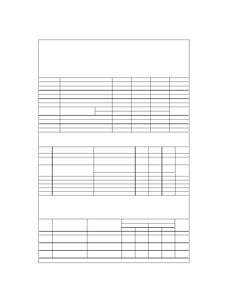
Absolute Maximum Ratings
(Note 1)
Note 1: The "Absolute Maximum Ratings" are those values beyond which
the safety of the device cannot be guaranteed. The device should not be
operated at these limits. The parametric values defined in the Electrical
Characteristics tables are not guaranteed at the absolute maximum ratings.
The "Recommended Operating Conditions" tables will define the conditions
for actual device operation.
Recommended Operating Conditions
Note 2: T
A
=
25
∞
C and V
CC
=
5V.
Electrical Characteristics
over recommended operating free air temperature range (unless otherwise noted)
Note 3: All typicals are at V
CC
=
5V, T
A
=
25
∞
C.
Note 4: Not more than one output should be shorted at a time, and the duration should not exceed one second.
Note 5: I
CC
is measured with all outputs OPEN, the SERIAL input grounded, the CLOCK input at 2.4V, and a momentary ground, then 4.5V, applied to the
CLEAR input.
Switching Characteristics
at V
CC
=
5V and T
A
=
25
∞
C
Supply Voltage
7V
Input Voltage
7V
Operating Free Air Temperature Range
0
∞
C to
+
70
∞
C
Storage Temperature Range
-
65
∞
C to
+
150
∞
C
Symbol
Parameter
Min
Nom
Max
Units
V
CC
Supply Voltage
4.75
5
5.25
V
V
IH
HIGH Level Input Voltage
2
V
V
IL
LOW Level Input Voltage
0.8
V
I
OH
HIGH Level Output Current
-
0.4
mA
I
OL
LOW Level Output Current
8
mA
f
CLK
Clock Frequency (Note 2)
0
25
MHz
t
W
Pulse Width
Clock
20
ns
(Note 2)
Clear
20
t
SU
Data Setup Time (Note 2)
17
ns
t
H
Data Hold Time (Note 2)
5
ns
t
REL
Clear Release Time (Note 2)
30
ns
T
A
Free Air Operating Temperature
0
70
∞
C
Symbol
Parameter
Conditions
Min
Typ
(Note 3)
Max
Units
V
I
Input Clamp Voltage
V
CC
=
Min, I
I
=
-
18 mA
-
1.5
V
V
OH
HIGH Level
V
CC
=
Min, I
OH
=
Max
2.7
3.4
V
Output Voltage
V
IL
=
Max, V
IH
=
Min
V
OL
LOW
Level V
CC
=
Min, I
OL
=
Max
0.35
0.5
Output Voltage
V
IL
=
Max, V
IH
=
Min
V
I
OL
=
4 mA, V
CC
=
Min
0.25
0.4
I
I
Input Current @ Max Input Voltage
V
CC
=
Max, V
I
=
7V
0.1
mA
I
IH
HIGH Level Input Current
V
CC
=
Max, V
I
=
2.7V
20
µ
A
I
IL
LOW Level Input Current
V
CC
=
Max, V
I
=
0.4V
-
0.4
mA
I
OS
Short Circuit Output Current
V
CC
=
Max (Note 4)
-
20
-
100
mA
I
CC
Supply Current
V
CC
=
Max (Note 5)
16
27
mA
From (Input)
R
L
=
2 k
Symbol
Parameter
To (Output)
C
L
=
15 pF
C
L
=
50 pF
Units
Min
Max
Min
Max
f
MAX
Maximum Clock Frequency
25
MHz
t
PLH
Propagation Delay Time
Clock to Output
27
30
ns
LOW-to-HIGH Level Output
t
PHL
Propagation Delay Time
Clock to Output
32
40
ns
HIGH-to-LOW Level Output
t
PHL
Propagation Delay Time
Clear to Output
36
45
ns
HIGH-to-LOW Level Output

www.fairchildsemi.com
4
DM74LS164
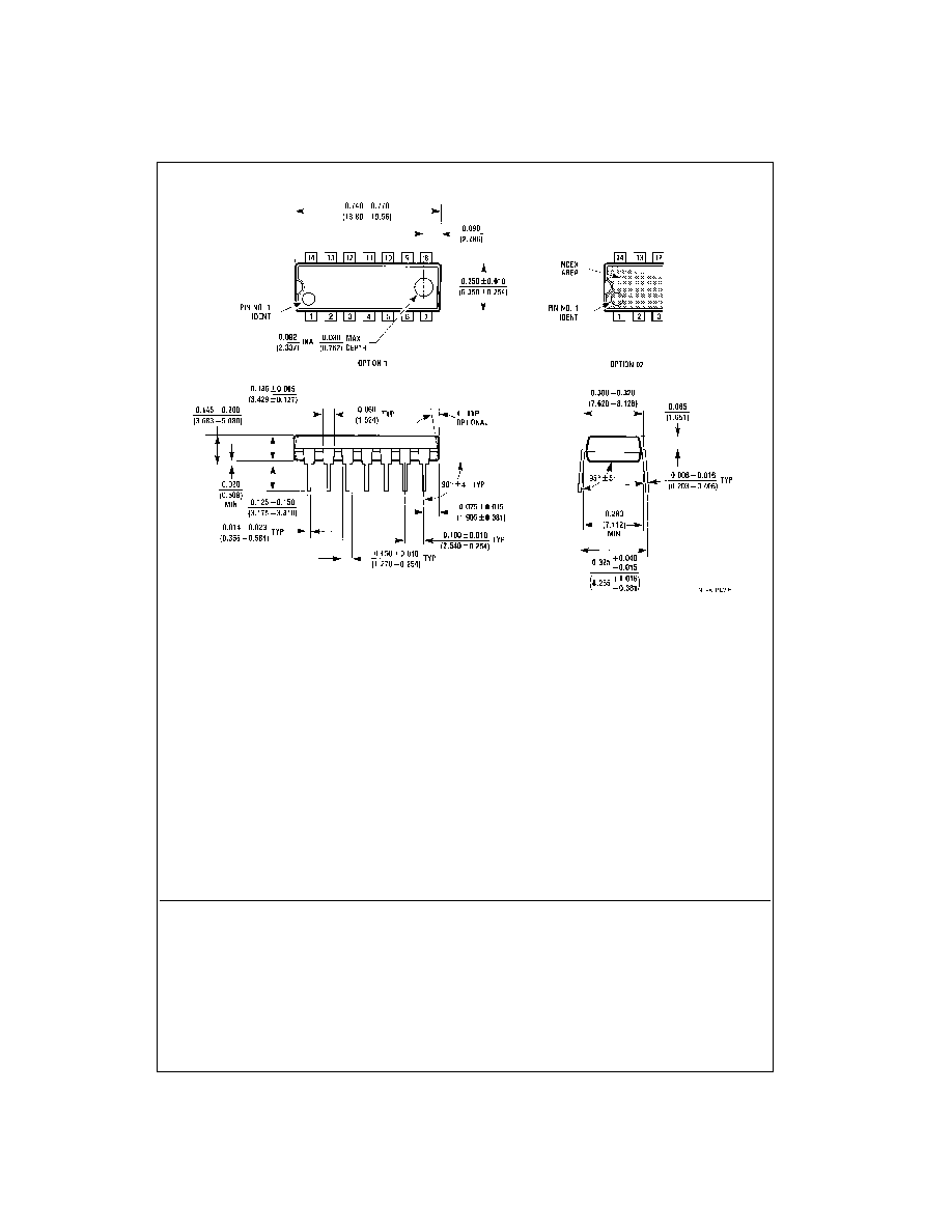
Physical Dimensions
inches (millimeters) unless otherwise noted
14-Lead Small Outline Integrated Circuit (SOIC), JEDEC MS-120, 0.150 Narrow
Package Number M14A
5
www.fairchildsemi.com
DM74LS164
8-
Bit
Ser
i
al
I
n
/Pa
r
al
lel
Out
Shi
f
t
Regi
ste
r
Physical Dimensions
inches (millimeters) unless otherwise noted (Continued)
14-Lead Plastic Dual-In-Line Package (PDIP), JEDEC MS-001, 0.300 Wide
Package Number N14A
Fairchild does not assume any responsibility for use of any circuitry described, no circuit patent licenses are implied and
Fairchild reserves the right at any time without notice to change said circuitry and specifications.
LIFE SUPPORT POLICY
FAIRCHILD'S PRODUCTS ARE NOT AUTHORIZED FOR USE AS CRITICAL COMPONENTS IN LIFE SUPPORT
DEVICES OR SYSTEMS WITHOUT THE EXPRESS WRITTEN APPROVAL OF THE PRESIDENT OF FAIRCHILD
SEMICONDUCTOR CORPORATION. As used herein:
1. Life support devices or systems are devices or systems
which, (a) are intended for surgical implant into the
body, or (b) support or sustain life, and (c) whose failure
to perform when properly used in accordance with
instructions for use provided in the labeling, can be rea-
sonably expected to result in a significant injury to the
user.
2. A critical component in any component of a life support
device or system whose failure to perform can be rea-
sonably expected to cause the failure of the life support
device or system, or to affect its safety or effectiveness.
www.fairchildsemi.com