 | –≠–ª–µ–∫—Ç—Ä–æ–Ω–Ω—ã–π –∫–æ–º–ø–æ–Ω–µ–Ω—Ç: 74LS573 | –°–∫–∞—á–∞—Ç—å:  PDF PDF  ZIP ZIP |

© 2000 Fairchild Semiconductor Corporation
DS009814
www.fairchildsemi.com
October 1988
Revised March 2000
DM74LS573
Octa
l D-T
ype Latch wit
h
3
-
ST
A
T
E
Outpu
t
s
DM74LS573
Octal D-Type Latch with 3-STATE Outputs
General Description
The DM74LS573 is a high speed octal latch with buffered
common Latch Enable (LE) and buffered common Output
Enable (OE) inputs.
This device is functionally identical to the DM74LS373, but
has different pinouts.
Features
s
Inputs and outputs on opposite sides of package allow-
ing easy interface with microprocessors
s
Useful as input or output port for microprocessors
s
Functionally identical to DM74LS373
s
Input clamp diodes limit high speed termination effects
s
Fully TTL and CMOS compatible
Ordering Code:
Devices also available in Tape and Reel. Specify by appending the suffix letter "X" to the ordering code.
Logic Symbol
V
CC
=
Pin 20
GND
=
Pin 10
Connection Diagram
Pin Descriptions
Function Tables
L
=
LOW State
H
=
HIGH State
X
=
Don't Care
Z
=
High Impedance State
Q
O
=
Previous Condition of O
Order Number
Package Number
Package Description
DM74LS573WM
M20B
20-Lead Small Outline Integrated Circuit (SOIC), JEDEC MS-013, 0.300 Wide
DM74LS573N
N20A
20-Lead Plastic Dual-In-Line Package (PDIP), JEDEC MS-001, 0.300 Wide
Pin Names
Description
D0≠D7
Data Inputs
LE
Latch Enable Input (Active HIGH)
OE
3-STATE Output Enable Input (Active LOW)
O0≠O7
3-STATE Latch Outputs
Output
Latch
D
Output
Enable
Enable
O
L
H
H
H
L
H
L
L
L
L
X
Q
O
H
X
X
Z

www.fairchildsemi.com
2
DM74LS573
Absolute Maximum Ratings
(Note 1)
Note 1: The "Absolute Maximum Ratings" are those values beyond which
the safety of the device cannot be guaranteed. The device should not be
operated at these limits. The parametric values defined in the Electrical
Characteristics tables are not guaranteed at the absolute maximum ratings.
The "Recommended Operating Conditions" table will define the conditions
for actual device operation.
Recommended Operating Conditions
Electrical Characteristics
Over recommended operating free air temperature range (unless otherwise noted)
Note 2: All typicals are at V
CC
=
5V, T
A
=
25
∞
C.
Note 3: Not more than one output should be shorted at a time, and the duration should not exceed one second.
Supply Voltage
7V
Input Voltage
7V
Operating Free Air Temperature Range
0
∞
C to
+
70
∞
C
Storage Temperature Range
-
65
∞
C to
+
150
∞
C
Symbol
Parameter
Min
Nom
Max
Units
V
CC
Supply Voltage
4.75
5
5.25
V
V
IH
HIGH Level Input Voltage
2
V
V
IL
LOW Level Input Voltage
0.8
V
I
OH
HIGH Level Input Current
-
2.6
mA
I
OL
LOW Level Output Current
24
mA
T
A
Free Air Operating Temperature
0
70
∞
C
Symbol
Parameter
Conditions
Min
Typ
Max
Units
(Note 2)
V
I
Input Clamp Voltage
V
CC
=
Min, I
I
=
-
18 mA
-
1.5
V
V
OH
HIGH Level
V
CC
=
Min, I
OH
=
Max,
2.7
3.4
V
Output Voltage
V
IL
=
Max
V
OL
LOW
Level V
CC
=
Min, I
OL
=
Max,
0.35
0.5
Output Voltage
V
IH
=
Min
V
I
OL
=
4 mA, V
CC
=
Min
0.25
0.4
I
I
Input Current @ Max Input Voltage
V
CC
=
Max, V
I
=
7V
1
mA
I
IH
HIGH Level Input Current
V
CC
=
Max, V
I
=
2.7V
20
µ
A
I
IL
LOW Level Input Current
V
CC
=
Max, V
I
=
0.4V
-
0.4
mA
I
OS
Short Circuit
V
CC
=
Max
-
30
-
130
mA
Output Current
(Note 3)
I
CC
Supply Current
V
CC
=
Max
50
mA
I
OZH
3-STATE Output
V
CC
=
V
CCH
20
µ
A
OFF Current HIGH
V
OZH
=
2.7V
I
OZL
3-STATE Output
V
CC
=
V
CCH
-
20
µ
A
OFF Current LOW
V
OZL
=
0.4V
3
www.fairchildsemi.com
DM74LS573
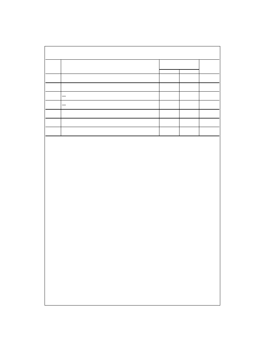
Switching Characteristics
at V
CC
=
5V and T
A
=
25
∞
C
R
L
=
2 k
,
Symbol
Parameter
C
L
=
50 pF
Units
Min
Max
t
PLH
Propagation Delay
27
ns
t
PHL
Data to Q
18
t
PLH
Propagation Delay
36
ns
t
PHL
LE to Q
25
t
PZH
3-STATE Enable Time
20
ns
t
PZL
OE to Q
25
t
PHZ
3-STATE Enable Time
20
ns
t
PLZ
OE to Q
25
t
S
(H)
Setup Time (HIGH/LOW)
3
ns
t
S
(L)
Data to LE
7
t
H
(H)
Hold Time (HIGH/LOW)
10
ns
t
H
(L)
Data to LE
10
t
W
(H)
Pulse Width (HIGH)
15
ns
Data to LE
www.fairchildsemi.com
4
DM74LS573
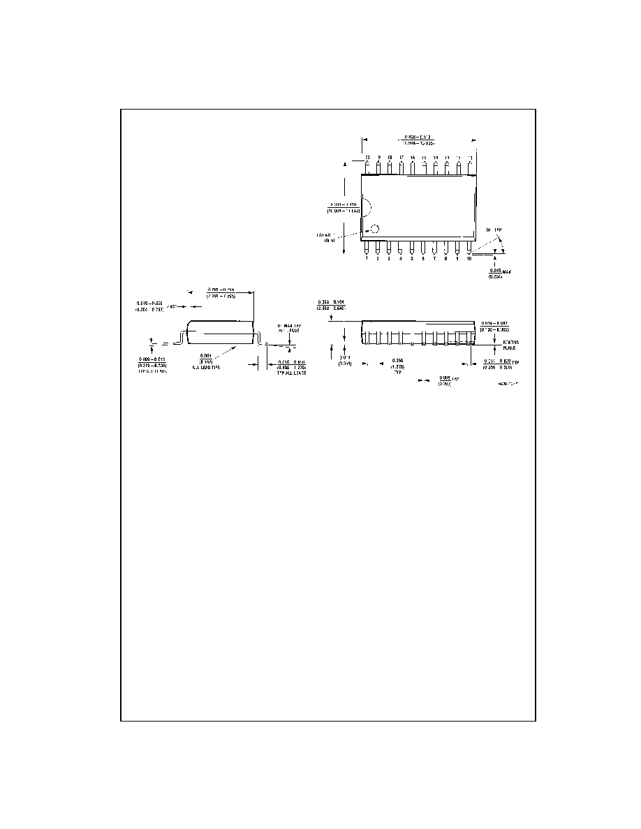
Physical Dimensions
inches (millimeters) unless otherwise noted
20-Lead Small Outline Integrated Circuit (SOIC), JEDEC MS-013, 0.300 Wide
Package Number M20B

5
www.fairchildsemi.com
DM74LS573
Octa
l D-T
ype Latch wit
h
3
-
ST
A
T
E
Outpu
t
s
Physical Dimensions
inches (millimeters) unless otherwise noted (Continued)
20-Lead Plastic Dual-In-Line Package (PDIP), JEDEC MS-001, 0.300 Wide
Package Number N20A
Fairchild does not assume any responsibility for use of any circuitry described, no circuit patent licenses are implied and
Fairchild reserves the right at any time without notice to change said circuitry and specifications.
LIFE SUPPORT POLICY
FAIRCHILD'S PRODUCTS ARE NOT AUTHORIZED FOR USE AS CRITICAL COMPONENTS IN LIFE SUPPORT
DEVICES OR SYSTEMS WITHOUT THE EXPRESS WRITTEN APPROVAL OF THE PRESIDENT OF FAIRCHILD
SEMICONDUCTOR CORPORATION. As used herein:
1. Life support devices or systems are devices or systems
which, (a) are intended for surgical implant into the
body, or (b) support or sustain life, and (c) whose failure
to perform when properly used in accordance with
instructions for use provided in the labeling, can be rea-
sonably expected to result in a significant injury to the
user.
2. A critical component in any component of a life support
device or system whose failure to perform can be rea-
sonably expected to cause the failure of the life support
device or system, or to affect its safety or effectiveness.
www.fairchildsemi.com