74LVQ125
Low Voltage Quad Buffer with 3-STATE Outputs
General Description
The LVQ125 contains four independent non-inverting buffers
with 3-STATE outputs.
Features
n
Ideal for low power/low noise 3.3V applications
n
Guaranteed simultaneous switching noise level and
dynamic threshold performance
n
Guaranteed pin-to-pin skew AC performance
n
Guaranteed incident wave switching into 75
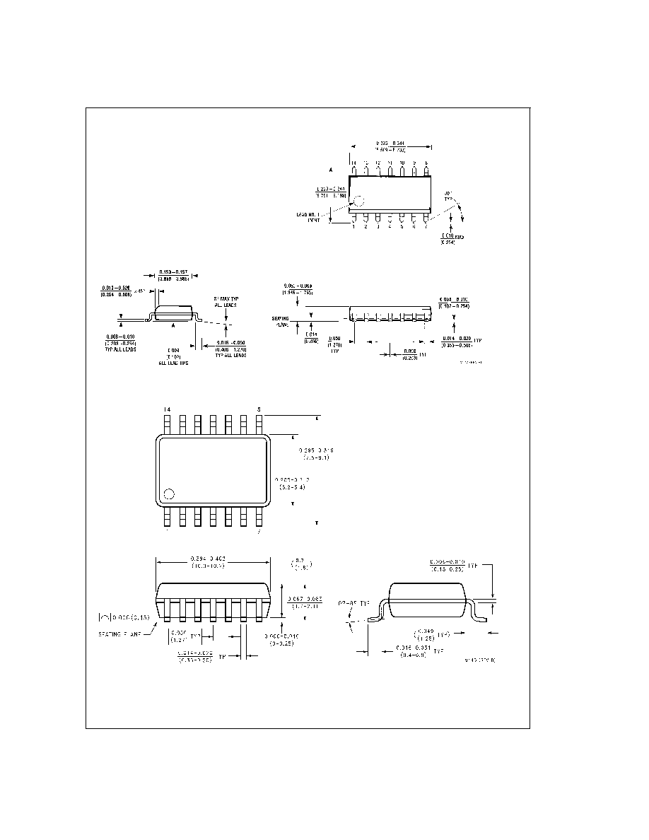
Ordering Code:
Order Number
Package Number
Package Description
74LVQ125SC
M14A
14-Lead (0.150" Wide) Small Outline Integrated Circuit, SOIC JEDEC
74LVQ125SJ
M14D
14-Lead Small Outline Package, SOIC EIAJ
Device also available in Tape and Reel. Specify by appending suffix letter "X" to the ordering code.
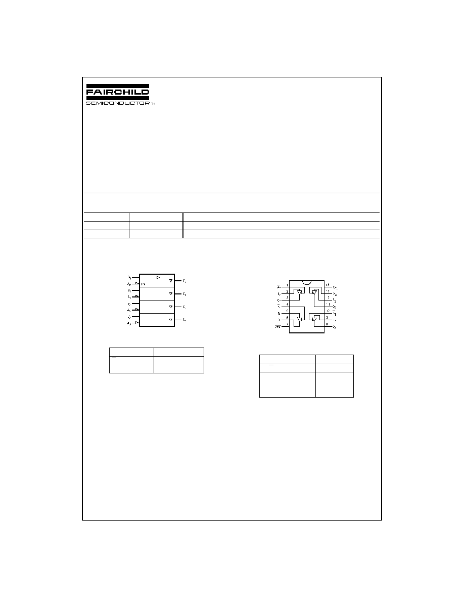
Logic Symbol
Pin Descriptions
Pin Names
Description
A
n
, B
n
Inputs
O
n
Outputs
Connection Diagram
Truth Table
Inputs
Output
A
n
B
n
O
n
L
L
L
L
H
H
H
X
Z
H = HIGH Voltage Level
L = LOW Voltage Level
Z = HIGH Impedance
X = Immaterial
IEEE/IEC
DS011349-1
Pin Assignment for
SOIC JEDEC and EIAJ
DS011349-2
May 1998
74L
VQ125
Low
V
oltage
Quad
Buffer
with
3-ST
A
T
E
Outputs
� 1998 Fairchild Semiconductor Corporation
DS011349
www.fairchildsemi.com

Absolute Maximum Ratings
(Note 1)
Supply Voltage (V
CC
)
-0.5V to +7.0V
DC Input Diode Current (I
IK
)
V
I
= -0.5V
-20 mA
V
I
= V
CC
+ 0.5V
+20 mA
DC Input Voltage (V
I
)
-0.5V to V
CC
+ 0.5V
DC Output Diode Current (I
OK
)
V
O
= -0.5V
-20 mA
V
O
= V
CC
+ 0.5V
+20 mA
DC Output Voltage (V
O
)
-0.5V to to V
CC
+ 0.5V
DC Output Source
or Sink Current (I
O
)
�
50 mA
DC V
CC
or Ground Current
(I
CC
or I
GND
)
�
200 mA
Storage Temperature (T
STG
)
-65�C to +150�C
DC Latch-Up Source or
Sink Current
�
100 mA
Recommended Operating
Conditions
(Note 2)
Supply Voltage (V
CC
)
2.0V to 3.6V
Input Voltage (V
I
)
0V to V
CC
Output Voltage (V
O
)
0V to V
CC
Operating Temperature (T
A
)
-40�C to +85�C
Minimum Input Edge Rate (
V/
t)
V
IN
from 0.8V to 2.0V
V
CC
@
3.0V
125 mV/ns
Note 1: The "Absolute Maximum Ratings" are those values beyond which
the safety of the device cannot be guaranteed. The device should not be op-
erated at these limits. The parametric values defined in the Electrical Charac-
teritics tables are not guaranteed at the absolute maximum ratings. The "Rec-
ommended Operating Conditions" table will define the conditions for actual
device operation.
Note 2: Unused inputs must be held HIGH or LOW. They may not float.
DC Electrical Characteristics
Symbol
Parameter
V
CC
(V)
T
A
= +25�C
T
A
= -40�C to +85� C
Units
Conditions
Typ
Guaranteed Limits
V
IH
Minimum High Level
Input Voltage
3.0
1.5
2.0
2.0
V
V
OUT
= 0.1V
or V
CC
- 0.1V
V
IL
Maximum Low Level
Input Voltage
3.0
1.5
0.8
0.8
V
V
OUT
= 0.1V
or V
CC
- 0.1V
V
OH
Minimum High Level
Output Voltage
3.0
2.99
2.9
2.9
V
I
OUT
= -50 �A
3.0
2.58
2.48
V
V
IN
= V
IL
or V
IH
(Note 3)
I
OH
= -12 mA
V
OL
Maximum Low Level
Output Voltage
3.0
0.002
0.1
0.1
V
I
OUT
= 50 �A
3.0
0.36
0.44
V
V
IN
= V
IL
or V
IH
(Note 3)
I
OL
= 12 mA
I
IN
Maximum Input
Leakage Current
3.6
�
0.1
�
1.0
�A
V
I
= V
CC
, GND
I
OZ
Maximum 3-STATE
Leakage Current
V
I
(OE) = V
IL
, V
IH
3.6
�
0.25
�
2.5
�A
V
I
= V
CC
, GND
V
O
= V
CC
, GND
I
OLD
Minimum Dynamic (Note 4)
Output Current
3.6
36
mA
V
OLD
= 0.8V Min (Note 5)
I
OHD
3.6
-25
mA
V
OHD
= 2.0V Min (Note 5)
I
CC
Maximum Quiescent
Supply Current
3.6
4.0
40.0
�A
V
IN
= V
CC
or GND
V
OLP
Quiet Output
Maximum Dynamic V
OL
3.3
0.6
1.0
V
(Notes 6, 7)
V
OLV
Quiet Output
Minimum Dynamic V
OL
3.3
-0.6
-1.0
V
(Notes 6, 7)
V
IHD
Maximum High Level
Dynamic Input Voltage
3.3
1.7
2.0
V
(Notes 6, 8)
V
ILD
Maximum Low Level
Dynamic Input Voltage
3.3
1.5
0.8
V
(Notes 6, 8)
Note 3: All outputs loaded; thresholds on input associated with output under test.
Note 4: Maximum test duration 2.0 ms, one output loaded at a time.
Note 5: Incident wave switching on transmission lines with impedances as low as 75
for commercial temperature range is guaranteed for 74LVQ.
Note 6: Worst case package.
Note 7: Max number of outputs defined as (n). Data inputs are driven 0V to 3.3V; one output at GND.
Note 8: Max number of Data Inputs (n) switching. (n - 1) inputs switching 0V to 3.3V. Input-under-test switching: 3.3V to threshold (V
ILD
), 0V to threshold (V
IHD
),
f = 1 MHz.
www.fairchildsemi.com
2

AC Electrical Characteristics
Symbol
Parameter
V
CC
(V)
T
A
= +25�C
C
L
= 50 pF
T
A
= -40�C to +85�C
C
L
= 50 pF
Units
Min
Typ
Max
Min
Max
t
PLH
Propagation Delay
2.7
1.0
7.8
12.7
1.0
14.0
ns
Data to Output
3.3
�
0.3
1.0
6.5
9.0
1.0
10.0
t
PHL
Propagation Delay
2.7
1.0
7.8
12.7
1.0
14.0
ns
Data to Output
3.3
�
0.3
1.0
6.5
9.0
1.0
10.0
t
PZH
Output Enable Time
2.7
1.0
7.2
14.8
1.0
16.0
ns
3.3
�
0.3
1.0
6.0
10.5
1.0
11.0
t
PZL
Output Enable Time
2.7
1.0
9.0
14.0
1.0
16.0
ns
3.3
�
0.3
1.0
7.5
10.0
1.0
11.0
t
PHZ
Output Disable Time
2.7
1.0
9.0
14.0
1.0
15.0
ns
3.3
�
0.3
1.0
7.5
10.0
1.0
10.5
t
PLZ
Output Disable Time
2.7
1.0
9.0
14.8
1.0
16.5
ns
3.3
�
0.3
1.0
7.5
10.5
1.0
11.5
t
OSHL,
Output to Output Skew (Note 9)
2.7
1.0
1.5
1.5
ns
t
OSLH
Data to Output
3.3
�
0.3
1.0
1.5
1.5
Note 9: Skew is defined as the absolute value of the difference between the actual propagation delay for any two separate outputs of the same device. The speci-
fication applies to any outputs switching in the same direction, either HIGH to LOW (t
OSHL
) or LOW to HIGH (t
OSLH
). Parameter guaranteed by design.
Capacitance
Symbol
Parameter
Typ
Units
Conditions
C
IN
Input Capacitance
4.5
pF
V
CC
= Open
C
PD
(Note 10)
Power Dissipation Capacitance
34
pF
V
CC
= 3.3V
Note 10: C
PD
is measured at 10 MHz.
3
www.fairchildsemi.com