
74LVQ138
Low Voltage 1-of-8 Decoder/Demultiplexer
General Description
The LVQ138 is a high-speed 1-of-8 decoder/demultiplexer.
This device is ideally suited for high-speed bipolar memory
chip select address decoding. The multiple input enables al-
low parallel expansion to a 1-of-24 decoder using just three
LVQ138 devices or a 1-of-32 decoder using four LVQ138 de-
vices and one inverter.
Features
n
Ideal for low power/low noise 3.3V applications
n
Guaranteed simultaneous switching noise level and
dynamic threshold performance
n
Improved latch-up immunity
n
Guaranteed incident wave switching into 75
n
4 kV minimum ESD immunity
n
Demultiplexing capability
n
Multiple input enable for each expansion
n
Active LOW mutually exclusive outputs
Ordering Code:
Order Number
Package Number
Package Description
74LVQ138SC
M16A
16-Lead (0.150" Wide) Small Outline Integrated Circuit, SOIC JEDEC
74LVQ138SJ
M16D
16-Lead Molded Small Outline Package, SOIC EIAJ
Devices also available in Tape and Reel. Specify by appending suffix letter "X" to the ordering code.
Logic Symbols
Connection Diagram
Pin Descriptions
Pin Names
Description
A
0
≠A
2
Address Inputs
E
1
≠E
2
Enable Inputs
E
3
Enable Input
O
0
≠O
7
Outputs
DS011350-1
IEEE/IEC
DS011350-4
Pin Assignment
for SOIC JEDEC and EIAJ
DS011350-2
May 1998
74L
VQ138
Low
V
oltage
1-of-8
Decoder/Demultiplexer
© 1998 Fairchild Semiconductor Corporation
DS011350
www.fairchildsemi.com

Functional Description
The LVQ138 high-speed 1-of-8 decoder/demultiplexer ac-
cepts three binary weighted inputs (A
0
, A
1
, A
2
) and, when
enabled, provides eight mutually exclusive active-LOW out-
puts (O
0
≠O
7
). The LVQ138 features three Enable inputs, two
active-LOW (E
1
, E
2
) and one active-HIGH (E
3
). All outputs
will be HIGH unless E
1
and E
2
are LOW and E
3
is HIGH.
This multiple enable function allows easy parallel expansion
of the device to a 1-of-32 (5 lines to 32 lines) decoder with
just four LVQ138 devices and one inverter (see
Figure 1).
The LVQ138 can be used as an 8-output demultiplexer by
using one of the active LOW Enable inputs as the data input
and the other Enable inputs as strobes. The Enable inputs
which are not used must be permanently tied to their appro-
priate active-HIGH or active-LOW state.
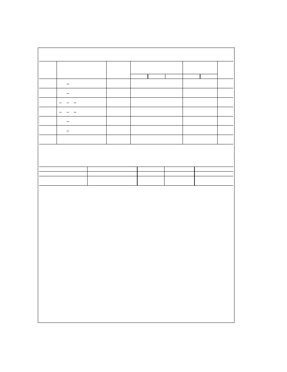
Truth Table
Inputs
Outputs
E
1
E
2
E
3
A
0
A
1
A
2
O
0
O
1
O
2
O
3
O
4
O
5
O
6
O
7
H
X
X
X
X
X
H
H
H
H
H
H
H
H
X
H
X
X
X
X
H
H
H
H
H
H
H
H
X
X
L
X
X
X
H
H
H
H
H
H
H
H
L
L
H
L
L
L
L
H
H
H
H
H
H
H
L
L
H
H
L
L
H
L
H
H
H
H
H
H
L
L
H
L
H
L
H
H
L
H
H
H
H
H
L
L
H
H
H
L
H
H
H
L
H
H
H
H
L
L
H
L
L
H
H
H
H
H
L
H
H
H
L
L
H
H
L
H
H
H
H
H
H
L
H
H
L
L
H
L
H
H
H
H
H
H
H
H
L
H
L
L
H
H
H
H
H
H
H
H
H
H
H
L
H = HIGH Voltage Level
L = LOW Voltage Level
X = Immaterial
Logic Diagram
DS011350-5
Please note that this diagram is provided only for the understanding of logic operations and should not be used to estimate propagation delays.
www.fairchildsemi.com
2
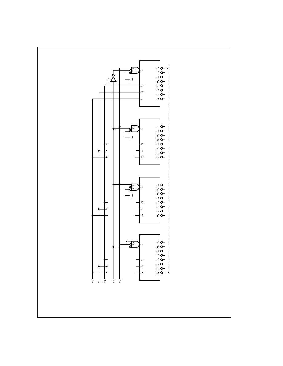
Logic Diagram
DS01
1350-6
FIGURE
1.
Expansion
to
1-of-32
Decoding
3
www.fairchildsemi.com

Absolute Maximum Ratings
(Note 1)
Supply Voltage (V
CC
)
-0.5V to +7.0V
DC Input Diode Current (I
IK
)
V
I
= -0.5V
-20 mA
V
I
= V
CC
+ 0.5V
+20 mA
DC Input Voltage (V
I
)
-0.5V to V
CC
+ 0.5V
DC Output Diode Current (I
OK
)
V
O
= -0.5V
-20 mA
V
O
= V
CC
+ 0.5V
+20 mA
DC Output Voltage (V
O
)
-0.5V to V
CC
+ 0.5V
DC Output Source
or Sink Current (I
O
)
±
50 mA
DC V
CC
or Ground Current
(I
CC
or I
GND
)
±
200 mA
Storage Temperature (T
STG
)
-65∞C to +150∞C
DC Latch-Up Source or
Sink Current
±
300 mA
Recommended Operating
Conditions
(Note 2)
Supply Voltage (V
CC
)
2.0V to 3.6V
Input Voltage (V
I
)
0V to V
CC
Output Voltage (V
O
)
0V to V
CC
Operating Temperature (T
A
)
-40∞C to +85∞C
Minimum Input Edge Rate (
V/
t)
V
IN
from 0.8V to 2.0V
V
CC
@
3.0V
125 mV/ns
Note 1: The "Absolute Maximum Ratings" are those values beyond which
the safety of the device cannot be guaranteed. The device should not be op-
erated at these limits. The parametric values defined in the Electrical Charac-
teristics tables are not guaranteed at the absolute maximum ratings. The
"Recommended Operating Conditions" table will define the conditions for ac-
tual device operation.
Note 2: Unused inputs must be held HIGH or LOW. They may not float.
DC Electrical Characteristics
Symbol
Parameter
V
CC
(V)
T
A
= +25∞C
T
A
= -40∞C to +85∞C
Units
Conditions
Typ
Guaranteed Limits
V
IH
Minimum High Level
3.0
1.5
2.0
2.0
V
V
OUT
= 0.1V
Input Voltage
or V
CC
- 0.1V
V
IL
Maximum Low Level
3.0
1.5
0.8
0.8
V
V
OUT
= 0.1V
Input Voltage
or V
CC
- 0.1V
V
OH
Minimum High Level
Output Voltage
3.0
2.99
2.9
2.9
V
I
OUT
= -50 µA
3.0
2.58
2.48
V
V
IN
= V
IL
or V
IH
(Note 3)
I
OH
= -12 mA
V
OL
Maximum Low Level
Outut Voltage
3.0
0.002
0.1
0.1
V
I
OUT
= 50 µA
3.0
0.36
0.44
V
V
IN
= V
IL
or V
IH
(Note 3)
I
OL
= 12 mA
I
IN
Maximum Input
3.6
±
0.1
±
1.0
µA
V
I
= V
CC
, GND
Leakage Current
I
OLD
Minimum Dynamic (Note 4)
3.6
36
mA
V
OLD
= 0.8V Max (Note 5)
I
OH
Output Current
3.6
-25
mA
V
OHD
= 2.0V Min (Note 5)
I
CC
Maximum Quiescent
3.6
4.0
40.0
µA
V
IN
= V
CC
Supply Current
or GND
V
OLP
Quiet Output
3.3
0.8
V
(Notes 6, 7)
Maximum Dynamic V
OL
V
OLV
Quiet Output
3.3
-0.8
V
(Notes 6, 7)
Minimum Dynamic V
OL
V
IHD
Maximum High Level
3.3
1.7
2.0
V
(Notes 6, 8)
Dynamic Input Voltage
V
ILD
Maximum Low Level
3.3
1.7
0.8
V
(Notes 6, 8)
Dynamic Input Voltage
Note 3: All outputs loaded; thresholds on input associated with output under test.
Note 4: Maximum test duration 2.0 ms, one output loaded at a time.
Note 5: Incident wave switching on transmission lines with impedances as low as 75
for commercial temperature range is guaranteed.
Note 6: Worst case package.
Note 7: Max number of outputs defined as (n). Data inputs are driven 0V to 3.3V; one output at GND.
Note 8: Max number of Data Inputs (n) switching. (n - 1) inputs switching 0V to 3.3V. Input-under-test switching: 3.3V to threshold (V
ILD
), 0V to threshold
(V
IHD
), f = 1 MHz.
www.fairchildsemi.com
4
AC Electrical Characteristics
Symbol
Parameter
V
CC
(V)
T
A
= +25∞C
C
L
= 50 pF
T
A
= -40∞C to +85∞C
C
L
= 50 pF
Units
Min
Typ
Max
Min
Max
t
PLH
Propagation Delay
2.7
1.5
10.2
18.3
1.5
21.0
ns
A
n
to O
n
3.3
±
0.3
1.5
8.5
13.0
1.5
15.0
t
PHL
Propagation Delay
2.7
1.5
9.6
17.6
1.5
20.0
ns
A
n
to O
n
3.3
±
0.3
1.5
8.0
12.5
1.5
14.0
t
PLH
Propagation Delay
2.7
1.5
13.2
21.0
1.5
23.0
ns
E
1
or E
2
to O
n
3.3
±
0.3
1.5
11.0
15.0
1.5
16.0
t
PHL
Propagation Delay
2.7
1.5
11.4
19.0
1.5
21.0
ns
E
1
or E
2
to O
n
3.3
±
0.3
1.5
9.5
13.5
1.5
15.0
t
PLH
Propagation Delay
2.7
1.5
13.2
21.8
1.5
23.5
ns
E
3
to O
n
3.3
±
0.3
1.5
11.0
15.5
1.5
16.5
t
PHL
Propagation Delay
2.7
1.5
10.2
18.3
1.5
20.0
ns
E
3
to O
n
3.3
±
0.3
1.5
8.5
13.0
1.5
14.0
t
OSHL,
Output to Output Skew (Note 9)
2.7
1.0
1.5
1.5
ns
t
OSLH
Data to Output
3.3
±
0.3
1.0
1.5
1.5
Note 9: Skew is defined as the absolute value of the difference between the actual propagation delay for any two separate outputs of the same device. The speci-
fication applies to any outputs switching in the same direction, either HIGH to LOW (t
OSHL
) or LOW to HIGH (t
OSLH
). Parameter guaranteed by design.
Capacitance
Symbol
Parameter
Typ
Units
Conditions
C
IN
Input Capacitance
4.5
pF
V
CC
= Open
C
PD
(Note 10)
Power Dissipation
45
pF
V
CC
= 3.3V
Capacitance
Note 10: C
PD
is measured at 10 MHz.
5
www.fairchildsemi.com