© 2001 Fairchild Semiconductor Corporation
DS011361
www.fairchildsemi.com
February 1992
Revised June 2001
7
4
L
V
Q573 Low
V
o
l
t
age Octa
l Latch wit
h
3
-
ST
A
T
E
Output
s
74LVQ573
Low Voltage Octal Latch with 3-STATE Outputs
General Description
The LVQ573 is a high-speed octal latch with buffered com-
mon Latch Enable (LE) and buffered common Output
Enable (OE) inputs. The LVQ573 is functionally identical to
the LVQ373 but with inputs and outputs on opposite sides
of the package.
Features
s
Ideal for low power/low noise 3.3V applications
s
Implements patented EMI reduction circuitry
s
Available in SOIC JEDEC, SOIC EIAJ, and QSOP
packages
s
Guaranteed simultaneous switching noise level
and dynamic threshold performance
s
Improved latch-up immunity
s
Guaranteed incident wave switching into 75
s
4 kV minimum ESD immunity
Ordering Code:
Devices also available in Tape and Reel. Specify by appending suffix letter "X" to the ordering code.
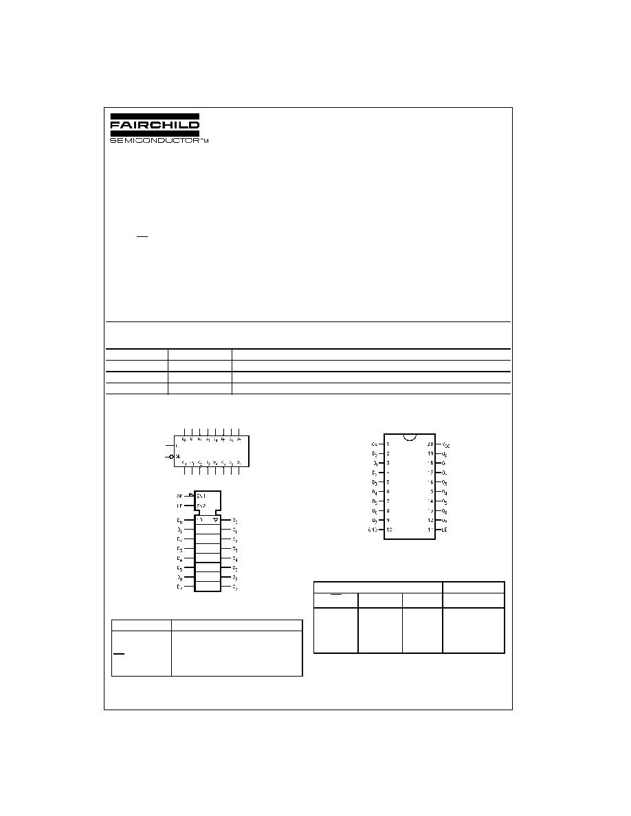
Logic Symbols
IEEE/IEC
Pin Descriptions
Connection Diagram
Truth Table
H
=
HIGH Voltage
L
=
LOW Voltage
Z
=
High Impedance
X
=
Immaterial
O
0
=
Previous O
0
before HIGH-to-LOW transition of Latch Enable
Order Number
Package Number
Package Description
74LVQ573SC
M20B
20-Lead Small Outline Integrated Circuit (SOIC), JEDEC MS-013, 0.300" Wide
74LVQ573SJ
M20D
20-Lead Small Outline Package (SOP), EIAJ TYPE II, 5.3mm Wide
74LVQ573QSC
MQA20
20-Lead Quarter Size Outline Package (QSOP), JEDEC MO-137, 0.150" Wide
Pin Names
Description
D
0
≠D
7
Data Inputs
LE
Latch Enable Input
OE
3-STATE Output Enable Input
O
0
≠O
7
3-STATE Latch Outputs
Inputs
Outputs
OE
LE
D
O
n
L
H
H
H
L
H
L
L
L
L
X
O
0
H
X
X
Z
www.fairchildsemi.com
2
74L
VQ
573
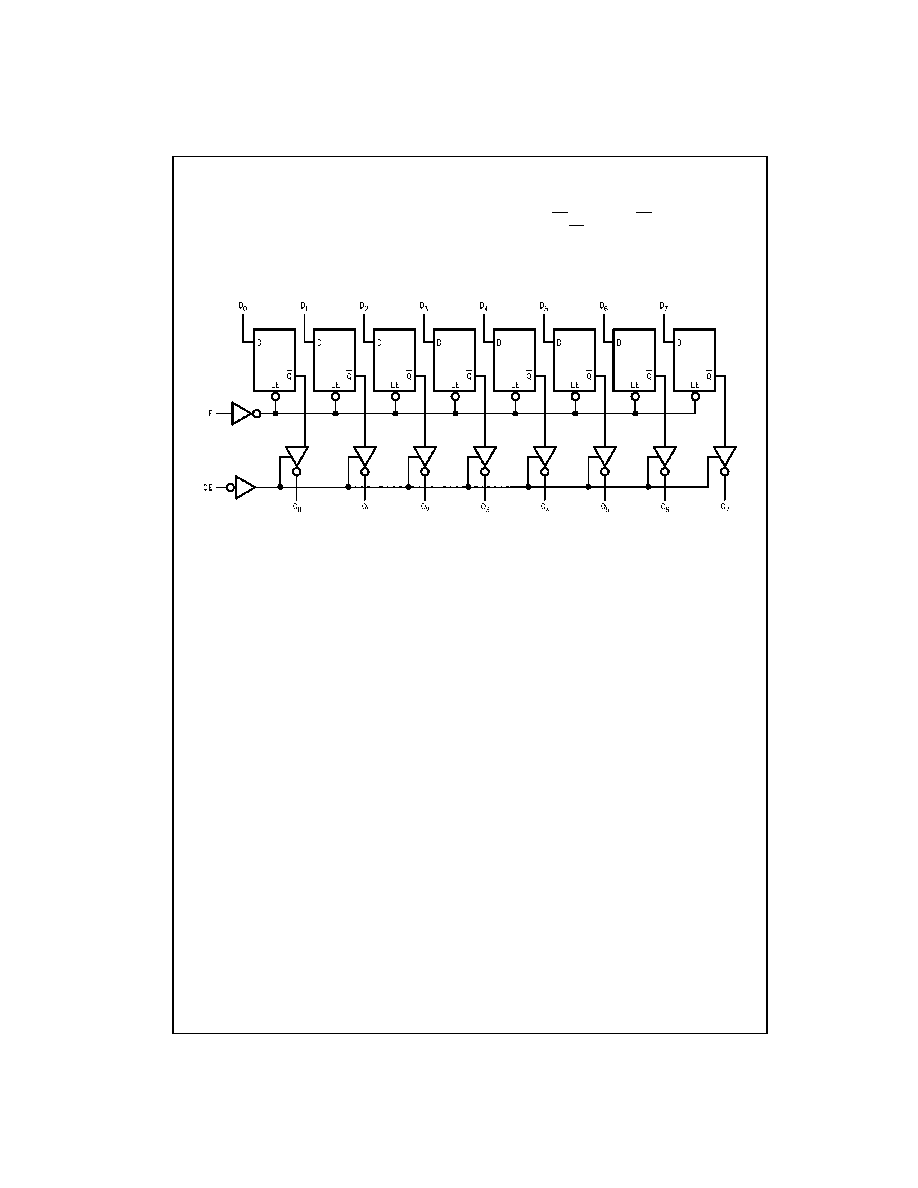
Functional Description
The LVQ573 contains eight D-type latches with 3-STATE
output buffers. When the Latch Enable (LE) input is HIGH,
data on the D
n
inputs enters the latches. In this condition
the latches are transparent, i.e., a latch output will change
state each time its D-type input changes. When LE is LOW
the latches store the information that was present on the
D-type inputs a setup time preceding the HIGH-to-LOW
transition of LE. The 3-STATE buffers are controlled by the
Output Enable (OE) input. When OE is LOW, the buffers
are enabled. When OE is HIGH the buffers are in the high
impedance mode but this does not interfere with entering
new data into the latches.
Logic Diagram
Please note that this diagram is provided only for the understanding of logic operations and should not be used to estimate propagation delays.

3
www.fairchildsemi.com
7
4
L
V
Q573
Absolute Maximum Ratings
(Note 1)
Recommended Operating
Conditions
(Note 2)
Note 1: The "Absolute Maximum Ratings" are those values beyond which
the safety of the device cannot be guaranteed. The device should not be
operated at these limits. The parametric values defined in the Electrical
Characteristics tables are not guaranteed at the absolute maximum ratings.
The "Recommended Operating Conditions" table will define the conditions
for actual device operation.
Note 2: Unused inputs must be held HIGH or LOW. They may not float.
DC Electrical Characteristics
Note 3: All outputs loaded; thresholds on input associated with output under test.
Note 4: Maximum test duration 2.0 ms, one output loaded at a time.
Note 5: Incident wave switching on transmission lines with impedances as low as 75
for commercial temperature range is guaranteed for.
Note 6: Worst case package.
Note 7: Max number of outputs defined as (n). Data inputs are driven 0V to 3.3V; one output at GND.
Note 8: Max number of Data Inputs (n) switching. (n
-
1) inputs switching 0V to 3.3V. Input-under-test switching: 3.3V to threshold (V
ILD
), 0V to threshold
(V
IHD
), f
=
1 MHz.
Supply Voltage (V
CC
)
-
0.5V to
+
7.0V
DC Input Diode Current (I
IK
)
V
I
=
-
0.5V
-
20 mA
V
I
=
V
CC
+
0.5V
+
20 mA
DC Input Voltage (V
I
)
-
0.5V to V
CC
+
0.5V
DC Output Diode Current (I
OK
)
V
O
=
-
0.5V
-
20 mA
V
O
=
V
CC
+
0.5V
+
20 mA
DC Output Voltage (V
O
)
-
0.5V to V
CC
+
0.5V
DC Output Source
or Sink Current (I
O
)
±
50 mA
DC V
CC
or Ground
Current (I
CC
or I
GND
)
±
400 mA
Storage Temperature (T
STG
)
-
65
∞
C to
+
150
∞
C
DC Latch-Up Source or
Sink Current
±
300 mA
Supply Voltage (V
CC
)
2.0V to 3.6V
Input Voltage (V
I
)
0V to V
CC
Output Voltage (V
O
)
0V to V
CC
Operating Temperature (T
A
)
-
40
∞
C to
+
85
∞
C
Minimum Input Edge Rate (
V/
t)
V
IN
from 0.8V to 2.0V
V
CC
@ 3.0V
125 mV/ns
Symbol
Parameter
V
CC
T
A
=
+
25
∞
C
T
A
=
-
40
∞
C to
+
85
∞
C
Units
Conditions
(V)
Typ
Guaranteed Limits
V
IH
Minimum High Level
3.0
1.5
2.0
2.0
V
V
OUT
=
0.1V
Input Voltage
or V
CC
-
0.1V
V
IL
Maximum Low Level
3.0
1.5
0.8
0.8
V
V
OUT
=
0.1V
Input Voltage
or V
CC
-
0.1V
V
OH
Minimum High Level
3.0
2.99
2.9
2.9
V
I
OUT
=
-
50
µ
A
Output Voltage
3.0
2.58
2.48
V
V
IN
=
V
IL
or V
IH
(Note 3)
I
OH
=
-
12 mA
V
OL
Maximum Low Level
3.0
0.002
0.1
0.1
V
I
OUT
=
50
µ
A
Output Voltage
3.0
0.36
0.44
V
V
IN
=
V
IL
or V
IH
(Note 3)
I
OL
=
12 mA
I
IN
Maximum Input Leakage Current
3.6
±
0.1
±
1.0
µ
A
V
I
=
V
CC
, GND
I
OLD
Minimum Dynamic
3.6
36
mA
V
OLD
=
0.8 V
Max
(Note 5)
I
OHD
Output Current (Note 4)
3.6
-
25
mA
V
OHD
=
2.0V V
Min
(Note 5)
I
CC
Maximum Quiescent
3.6
4.0
40.0
µ
A
V
IN
=
V
CC
Supply Current
or GND
I
OZ
3-STATE
V
I
(OE)
=
V
IL
, V
IH
Leakage Current
3.6
±
0.25
±
2.5
µ
A
V
I
=
V
CC
, GND
V
O
=
V
CC
, GND
V
OLP
Quiet Output
Maximum Dynamic V
OL
3.3
0.4
0.8
V
(Note 6)(Note 7)
V
OLV
Quiet Output
Minimum Dynamic V
OL
3.3
-
0.4
-
0.8
V
(Note 6)(Note 7)
V
IHD
Maximum High Level
Dynamic Input Voltage
3.3
1.6
2.0
V
(Note 6)(Note 8)
V
ILD
Maximum Low Level
Dynamic Input Voltage
3.3
1.6
0.8
V
(Note 6)(Note 8)
www.fairchildsemi.com
4
74L
VQ
573
AC Electrical Characteristics
Note 9: Skew is defined as the absolute value of the difference between the actual propagation delay for any two separate outputs of the same device. The
specification applies to any outputs switching in the same direction, either HIGH-to-LOW (t
OSHL
) or LOW-to-HIGH (t
OSLH
). Parameter guaranteed by design.
AC Operating Requirements
Capacitance
Note 10: C
PD
is measured at 10 MHz.
Symbol
Parameter
T
A
=
+
25
∞
C
T
A
=
-
40
∞
C to
+
85
∞
C
Units
V
CC
C
L
=
50 pF
C
L
=
50 pF
(V)
Min
Typ
Max
Min
Max
t
PHL
Propagation Delay
2.7
2.5
10.2
14.8
2.5
16.0
ns
t
PLH
D
n
to O
n
3.3
±
0.3
2.5
8.5
10.5
2.5
11.0
t
PLH
Propagation Delay
2.7
2.5
10.2
16.9
2.5
18.0
ns
t
PHL
LE to O
n
3.3
±
0.3
2.5
8.5
12.0
2.5
12.5
t
PZL
Output Enable Time
2.7
2.5
10.2
18.3
2.5
19.0
ns
t
PZH
3.3
±
0.3
2.5
8.5
13.0
2.5
13.5
t
PHZ
Output Disable Time
2.7
1.0
10.8
20.4
1.0
21.0
ns
t
PLZ
3.3
±
0.3
1.0
9.0
14.5
1.0
15.0
t
OSHL
Output to Output Skew (Note 9)
2.7
1.0
1.5
1.5
ns
t
OSLH
D
n
to O
n
3.3
±
0.3
1.0
1.5
1.5
Symbol
Parameter
T
A
=
+
25
∞
C
T
A
=
-
40
∞
C to
+
85
∞
C
Units
V
CC
C
L
=
50 pF
C
L
=
50 pF
(V)
Typ
Guaranteed Minimum
t
S
Setup Time, HIGH or LOW
2.7
0
4.0
4.5
ns
D
n
to LE
3.3
±
0.3
0
3.0
3.0
t
H
Hold Time, HIGH or LOW
2.7
0
1.5
1.5
ns
D
n
to LE
3.3
±
0.3
0
1.5
1.5
t
W
LE Pulse Width, HIGH
2.7
2.4
5.0
6.0
ns
3.3
±
0.3
2.0
4.0
4.0
Symbol
Parameter
Typ
Units
Conditions
C
IN
Input Capacitance
4.5
pF
V
CC
=
Open
C
PD
(Note 10)
Power Dissipation Capacitance
37
pF
V
CC
=
3.3V
5
www.fairchildsemi.com
7
4
L
V
Q573
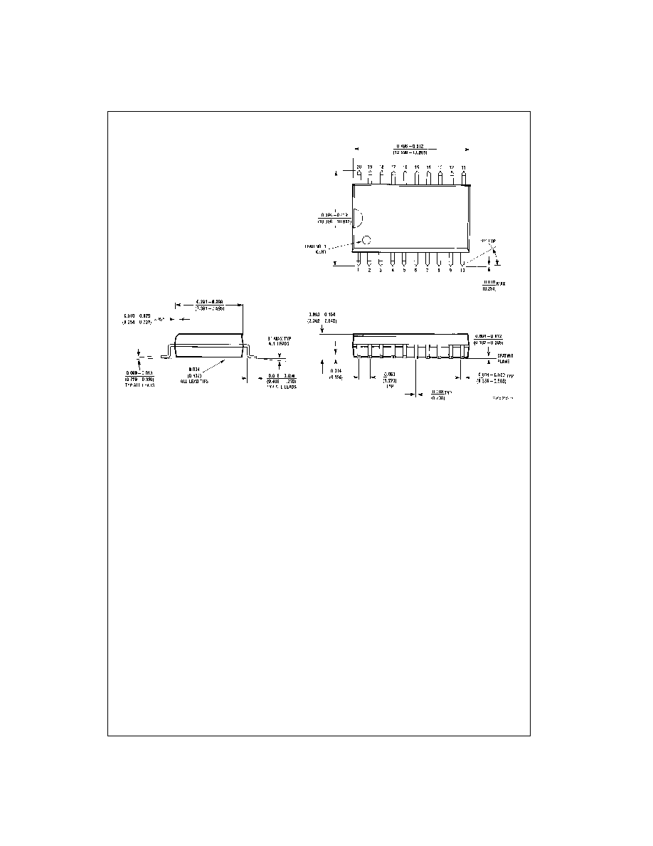
Physical Dimensions
inches (millimeters) unless otherwise noted
20-Lead Small Outline Integrated Circuit (SOIC), JEDEC MS-013, 0.300" Wide
Package Number M20B