© 2005 Fairchild Semiconductor Corporation
DS012011
www.fairchildsemi.com
October 1998
Revised February 2005
7
4
L
V
TH12
5 Low
V
o
l
t
age
Quad Buf
f
er
wi
th
3-ST
A
T
E Out
put
s
74LVTH125
Low Voltage Quad Buffer with 3-STATE Outputs
General Description
The LVTH125 contains four independent non-inverting
buffers with 3-STATE outputs.
These buffers are designed for low-voltage (3.3V) V
CC
applications, but with the capability to provide a TTL inter-
face to a 5V environment. The LVTH125 is fabricated with
an advanced BiCMOS technology to achieve high speed
operation similar to 5V ABT while maintaining a low power
dissipation.
Features
s
Input and output interface capability to systems at
5V V
CC
s
Bushold data inputs eliminate the need for external
pull-up resistors to hold unused inputs
s
Live insertion/extraction permitted
s
Power Up/Down high impedance provides glitch-free
bus loading
s
Outputs source/sink
32 mA/
64 mA
s
Functionally compatible with the 74 series 125
s
Latch-up performance exceeds 500 mA
s
ESD performance:
Human-body model
!
2000V
Machine model
!
200V
Charged-device model
!
1000V
Ordering Code:
Device also available in Tape and Reel. Specify by appending suffix letter "X" to the ordering code.
Pb-Free package per JEDEC J-STD-020B.
Note 1: "_NL" indicates Pb-Free package (per JEDED J-STD-020B). Device available in Tape and Reel only.
Order Number
Package
Package Description
Number
74LVTH125M
M14A
14-Lead Small Outline Integrated Circuit (SOIC), JEDEC MS-012, 0.150" Narrow
74LVTH125SJ
M14D
Pb-Free 14-Lead Small Outline Package (SOP), EIAJ TYPE II, 5.3mm Wide
74LVTH125MTC
MTC14
14-Lead Thin Shrink Small Outline Package (TSSOP), JEDEC MO-153, 4.4mm Wide
74LVTH125MTCX_NL
(Note 1)
MTC14
Pb-Free 14-Lead Thin Shrink Small Outline Package (TSSOP), JEDEC MO-153, 4.4mm
Wide
www.fairchildsemi.com
2
74
L
V
TH125
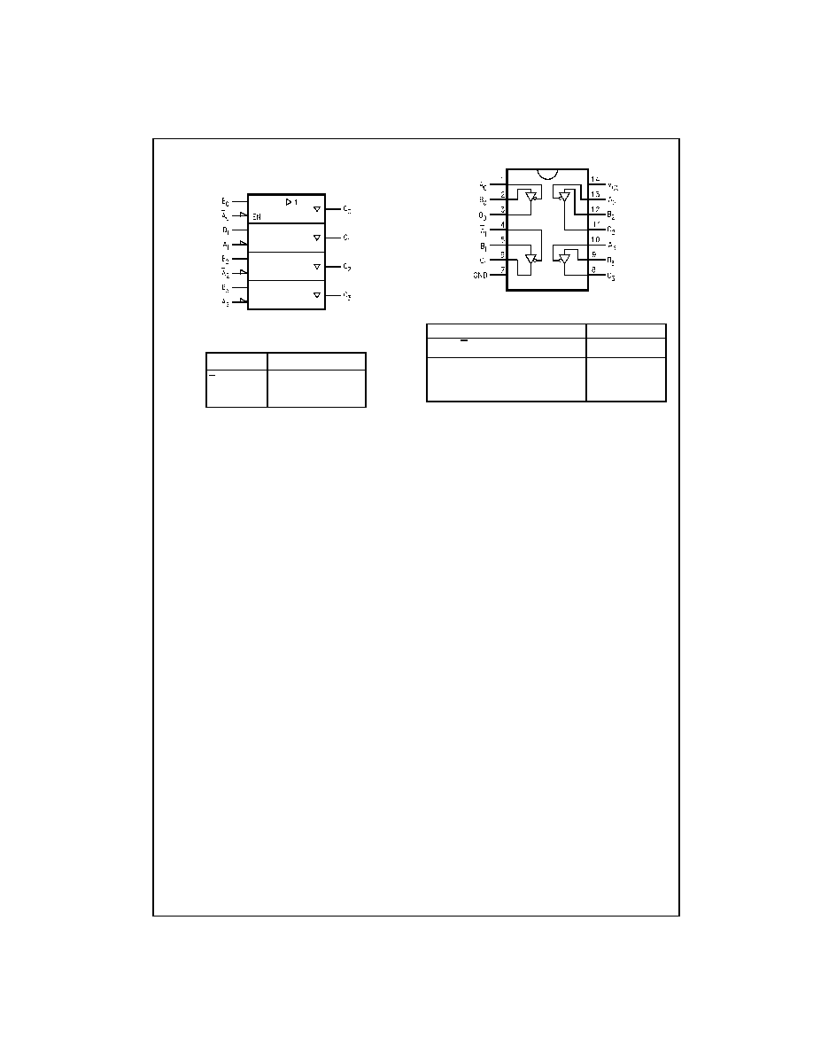
Logic Symbol
IEEE/IEC
Pin Descriptions
Connection Diagram
Truth Table
H
HIGH Voltage Level
L
LOW Voltage Level
X
Immaterial
Z
HIGH Impedance
Pin Names
Description
A
n
, B
n
Inputs
O
n
3-STATE Outputs
Inputs
Output
A
n
B
n
O
n
L
L
L
L
H
H
H
X
Z

3
www.fairchildsemi.com
7
4
L
V
TH12
5
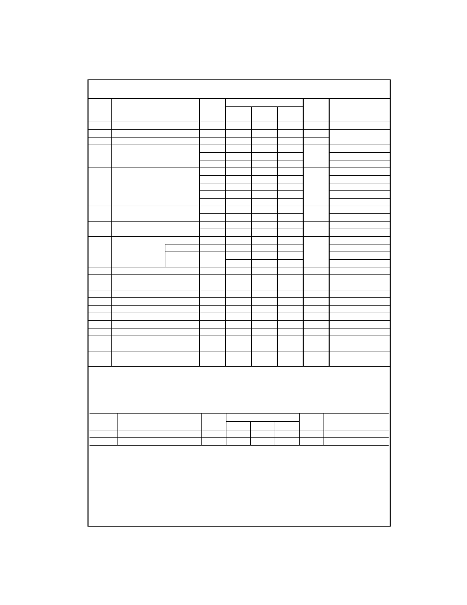
Absolute Maximum Ratings
(Note 2)
Recommended Operating Conditions
Note 2: Absolute Maximum continuous ratings are those values beyond which damage to the device may occur. Exposure to these conditions or conditions
beyond those indicated may adversely affect device reliability. Functional operation under absolute maximum rated conditions is not implied.
Note 3: I
O
Absolute Maximum Rating must be observed.
Symbol
Parameter
Value
Conditions
Units
V
CC
Supply Voltage
0.5 to
4.6
V
V
I
DC Input Voltage
0.5 to
7.0
V
V
O
DC Output Voltage
0.5 to
7.0
Output in 3-STATE
V
0.5 to
7.0
Output in HIGH or LOW State (Note 3)
I
IK
DC Input Diode Current
50
V
I
GND
mA
I
OK
DC Output Diode Current
50
V
O
GND
mA
I
O
DC Output Current
64
V
O
!
V
CC
Output at HIGH State
mA
128
V
O
!
V
CC
Output at LOW State
I
CC
DC Supply Current per Supply Pin
r
64
mA
I
GND
DC Ground Current per Ground Pin
r
128
mA
T
STG
Storage Temperature
65 to
150
q
C
Symbol
Parameter
Min
Max
Units
V
CC
Supply Voltage
2.7
3.6
V
V
I
Input Voltage
0
5.5
V
I
OH
HIGH Level Output Current
32
mA
I
OL
LOW Level Output Current
64
mA
T
A
Free-Air Operating Temperature
40
85
q
C
'
t/
'
V
Input Edge Rate, V
IN
0.8V ≠ 2.0V, V
CC
3.0V
0
10
ns/V
www.fairchildsemi.com
4
74
L
V
TH125
DC Electrical Characteristics
Note 4: All typical values are at V
CC
3.3V, T
A
25
q
C.
Note 5: An external driver must source at least the specified current to switch from LOW-to-HIGH.
Note 6: An external driver must sink at least the specified current to switch from HIGH-to-LOW.
Note 7: This is the increase in supply current for each input that is at the specified voltage level rather than V
CC
or GND.
Dynamic Switching Characteristics
(Note 8)
Note 8: Characterized in SOIC package. Guaranteed parameter, but not tested.
Note 9: Max number of outputs defined as (n). n
1 data inputs are driven 0V to 3V. Output under test held LOW.
Symbol
Parameter
V
CC
(V)
T
A
40
q
C to
85
q
C
Units
Conditions
Min
Typ
Max
(Note 4)
V
IK
Input Clamp Diode Voltage
2.7
1.2
V
I
I
18 mA
V
IH
Input HIGH Voltage
2.7≠3.6
2.0
V
V
O
d
0.1V or
V
IL
Input LOW Voltage
2.7≠3.6
0.8
V
V
O
t
V
CC
0.1V
V
OH
Output HIGH Voltage
2.7≠3.6
V
CC
0.2
V
I
OH
100
P
A
2.7
2.4
I
OH
8 mA
3.0
2.0
I
OH
32 mA
V
OL
Output LOW Voltage
2.7
0.2
V
I
OL
100
P
A
2.7
0.5
I
OL
24 mA
3.0
0.4
I
OL
16 mA
3.0
0.5
I
OL
32 mA
3.0
0.55
I
OL
64 mA
I
I(HOLD)
Bushold Input Minimum Drive
3.0
75
P
A
V
I
0.8V
75
V
I
2.0V
I
I(OD)
Bushold Input Over-Drive
3.0
500
P
A
(Note 5)
Current to Change State
500
(Note 6)
I
I
Input Current
3.6
10
P
A
V
I
5.5V
Control Pins
3.6
r
1
V
I
0V or V
CC
Data Pins
3.6
5
V
I
0V
1
V
I
V
CC
I
OFF
Power Off Leakage Current
0
r
100
P
A
0V
d
V
I
or V
O
d
5.5V
I
PU/PD
Power up/down 3-STATE
0≠1.5V
r
100
P
A
V
O
0.5V to 3.0V
Output Current
V
I
GND or V
CC
I
OZL
3-STATE Output Leakage Current
3.6
5
P
A
V
O
0.5V
I
OZH
3-STATE Output Leakage Current
3.6
5
P
A
V
O
3.0V
I
OZH
3-STATE Output Leakage Current
3.6
10
P
A
V
CC
V
O
d
5.5V
I
CCH
Power Supply Current
3.6
0.19
mA
Outputs HIGH
I
CCL
Power Supply Current
3.6
5
mA
Outputs LOW
I
CCZ
Power Supply Current
3.6
0.19
mA
Outputs Disabled
I
CCZ
Power Supply Current
3.6
0.19
mA
V
CC
d
V
O
d
5.5V
Outputs Disabled
'
I
CC
Increase in Power Supply Current
3.6
0.2
mA
One Input at V
CC
0.6V
(Note 7)
Other Inputs at V
CC
or GND
Symbol
Parameter
V
CC
T
A
25
q
C
Units
Conditions
(V)
Min
Typ
Max
C
L
50 pF, R
L
500
:
V
OLP
Quiet Output Maximum Dynamic V
OL
3.3
0.8
V
(Note 9)
V
OLV
Quiet Output Minimum Dynamic V
OL
3.3
0.8
V
(Note 9)

5
www.fairchildsemi.com
7
4
L
V
TH12
5
AC Electrical Characteristics
Note 10: All typical values are at V
CC
3.3V, T
A
25
q
C.
Note 11: Skew is defined as the absolute value of the difference between the actual propagation delay for any two separate outputs of the same device. The
specification applies to any outputs switching in the same direction, either HIGH-to-LOW (t
OSHL
) or LOW-to-HIGH (t
OSLH
).
Capacitance
(Note 12)
Note 12: Capacitance is measured at frequency f
1 MHz, per MIL-STD-883B, Method 3012.
Symbol
Parameter
T
A
40
q
C to
85
q
C
Units
C
L
50 pF, R
L
500
:
V
CC
3.3V
r
0.3V
V
CC
2.7V
Min
Typ
Max
Min
Max
(Note 10)
t
PLH
Propagation Delay Data to Output
1.0
3.5
1.0
4.5
ns
t
PHL
1.0
3.9
1.0
4.9
t
PZH
Output Enable Time
1.0
4.0
1.0
5.5
ns
t
PZL
1.1
4.0
1.1
5.4
t
PHZ
Output Disable Time
1.5
4.5
1.5
5.7
ns
t
PLZ
1.3
4.5
1.3
4.0
t
OSHL
Output to Output Skew
1.0
1.0
ns
t
OSLH
(Note 11)
Symbol
Parameter
Conditions
Typical
Units
C
IN
Input Capacitance
V
CC
0V, V
I
0V or V
CC
4
pF
C
OUT
Output Capacitance
V
CC
3.0V, V
O
0V or V
CC
8
pF