
© 2005 Fairchild Semiconductor Corporation
DS500355
www.fairchildsemi.com
June 2000
Revised June 2005
7
4
L
V
TH16
2374 L
o
w
V
o
lt
age
16-
Bit
D-
T
ype Fl
ip
-Fl
op wi
th
3-ST
A
T
E Out
put
s
and 25
:
Seri
es Resist
ors in
t
he
Out
put
s
74LVTH162374
Low Voltage 16-Bit D-Type Flip-Flop
with 3-STATE Outputs
and 25
:
Series Resistors in the Outputs
General Description
The LVTH162374 contains sixteen non-inverting D-type
flip-flops with 3-STATE outputs and is intended for bus ori-
ented applications. The device is byte controlled. A buff-
ered clock (CP) and Output Enable (OE) are common to
each byte and can be shorted together for full 16-bit opera-
tion.
The LVTH162374 is designed with equivalent 25
:
series
resistance in both the HIGH and LOW states of the output.
This design reduces line noise in applications such as
memory address drivers, clock drivers, and bus transceiv-
ers/transmitters.
The LVTH162374 data inputs include bushold, eliminating
the need for external pull-up resistors to hold unused
inputs.
These flip-flops are designed for low-voltage (3.3V) V
CC
applications, but with the capability to provide a TTL inter-
face to a 5V environment. The LVTH162374 is fabricated
with an advanced BiCMOS technology to achieve high
speed operation similar to 5V ABT while maintaining a low
power dissipation.
Features
s
Input and output interface capability to systems at
5V V
CC
s
Bushold data inputs eliminate the need for external
pull-up resistors to hold unused inputs
s
Live insertion/extraction permitted
s
Power Up/Power Down high impedance provides
glitch-free bus loading
s
Outputs include equivalent series resistance of 25
:
to
make external termination resistors unnecessary and
reduce overshoot and undershoot
s
Functionally compatible with the 74 series 16374
s
Latch-up performance exceeds 500 mA
s
ESD performance:
Human-body model
!
2000V
Machine model
!
200V
Charged-device model
!
1000V
s
Also packaged in plastic Fine-Pitch Ball Grid Array
(FBGA) (Preliminary)
Ordering Code:
Note 1: BGA package available in Tape and Reel only.
Order Number
Package
Number
Package Description
74LVTH162374GX
(Note 1)
BGA54A
(Preliminary)
54-Ball Fine-Pitch Ball Grid Array (FBGA), JEDEC MO-205, 5.5mm Wide
[TAPE and REEL]
74LVTH162374MEA
MS48A
48-Lead Small Shrink Outline Package (SSOP), JEDEC MO-118, 0.300" Wide
[TUBES]
74LVTH162374MEX
MS48A
48-Lead Small Shrink Outline Package (SSOP), JEDEC MO-118, 0.300" Wide
[TAPE and REEL]
74LVTH162374MTD
MTD48
48-Lead Thin Shrink Small Outline Package (TSSOP), JEDEC MO-153, 6.1mm Wide
[TUBES]
74LVTH162374MTX
MTD48
48-Lead Thin Shrink Small Outline Package (TSSOP), JEDEC MO-153, 6.1mm Wide
[TAPE and REEL]
www.fairchildsemi.com
2
74L
VTH162374
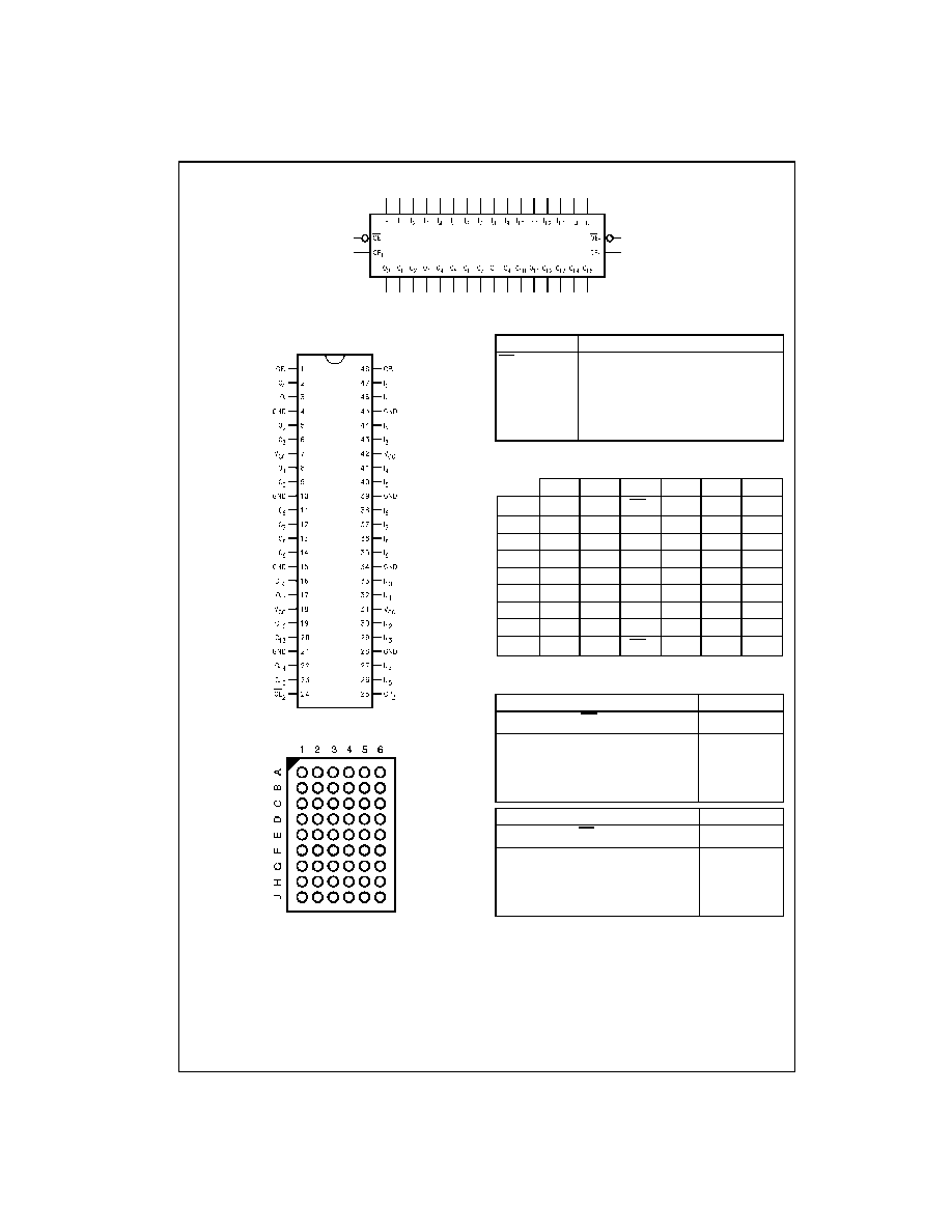
Logic Symbol
Connection Diagrams
Pin Assignments for SSOP and TSSOP
Pin Assignment for FBGA
(Top Thru View)
Pin Descriptions
FBGA Pin Assignments
Truth Tables
H
HIGH Voltage Level
L
LOW Voltage Level
X
Immaterial
Z
HIGH Impedance
O
o
Previous O
o
before HIGH-to-LOW of CP
Pin Names
Description
OE
n
Output Enable Input (Active LOW)
CP
n
Clock Pulse Input
I
0
≠I
15
Inputs
O
0
≠O
15
3-STATE Outputs
NC
No Connect
1
2
3
4
5
6
A
O
0
NC
OE
1
CP
1
NC
I
0
B
O
2
O
1
NC
NC
I
1
I
2
C
O
4
O
3
V
CC
V
CC
I
3
I
4
D
O
6
O
5
GND
GND
I
5
I
6
E
O
8
O
7
GND
GND
I
7
I
8
F
O
10
O
9
GND
GND
I
9
I
10
G
O
12
O
11
V
CC
V
CC
I
11
I
12
H
O
14
O
13
NC
NC
I
13
I
14
J
O
15
NC
OE
2
CP
2
NC
I
15
Inputs
Outputs
CP
1
OE
1
I
0
≠I
7
O
0
≠O
7
L
H
H
L
L
L
L
L
X
O
o
X
H
X
Z
Inputs
Outputs
CP
2
OE
2
I
8
≠I
15
O
8
≠O
15
L
H
H
L
L
L
L
L
X
O
o
X
H
X
Z

3
www.fairchildsemi.com
7
4
L
V
TH16
2374
Functional Description
The LVTH162374 consists of sixteen edge-triggered flip-flops with individual D-type inputs and 3-STATE true outputs. The
device is byte controlled with each byte functioning identically, but independent of the other. The control pins can be
shorted together to obtain full 16-bit operation. Each byte has a buffered clock and buffered Output Enable common to all
flip-flops within that byte. The description which follows applies to each byte. Each flip-flop will store the state of their indi-
vidual D-type inputs that meet the setup and hold time requirements on the LOW-to-HIGH Clock (CP
n
) transition. With the
Output Enable (OE
n
) LOW, the contents of the flip-flops are available at the outputs. When OE
n
is HIGH, the outputs go to
the high impedance state. Operation of the OE
n
input does not affect the state of the flip-flops.
Logic Diagrams
Byte 1 (0:7)
Byte 2 (8:15)
Please note that these diagrams are provided for the understanding of logic operation and should not be used to estimate propagation delays.

www.fairchildsemi.com
4
74L
VTH162374
Absolute Maximum Ratings
(Note 2)
Recommended Operating Conditions
Note 2: Absolute Maximum continuous ratings are those values beyond which damage to the device may occur. Exposure to these conditions or conditions
beyond those indicated may adversely affect device reliability. Functional operation under absolute maximum rated conditions is not implied.
Note 3: I
O
Absolute Maximum Rating must be observed.
DC Electrical Characteristics
Symbol
Parameter
Value
Conditions
Units
V
CC
Supply Voltage
0.5 to
4.6
V
V
I
DC Input Voltage
0.5 to
7.0
V
V
O
DC Output Voltage
0.5 to
7.0
Output in 3-STATE
V
0.5 to
7.0
Output in HIGH or LOW State (Note 3)
I
IK
DC Input Diode Current
50
V
I
GND
mA
I
OK
DC Output Diode Current
50
V
O
GND
mA
I
O
DC Output Current
64
V
O
!
V
CC
Output at HIGH State
mA
128
V
O
!
V
CC
Output at LOW State
I
CC
DC Supply Current per Supply Pin
r
64
mA
I
GND
DC Ground Current per Ground Pin
r
128
mA
T
STG
Storage Temperature
65 to
150
q
C
Symbol
Parameter
Min
Max
Units
V
CC
Supply Voltage
2.7
3.6
V
V
I
Input Voltage
0
5.5
V
I
OH
HIGH Level Output Current
12
mA
I
OL
LOW Level Output Current
12
mA
T
A
Free-Air Operating Temperature
40
85
q
C
'
t/
'
V
Input Edge Rate, V
IN
0.8V≠2.0V, V
CC
3.0V
0
10
ns/V
Symbol
Parameter
V
CC
T
A
40
q
C to
85
q
C
Units
Conditions
(V)
Min
Max
V
IK
Input Clamp Diode Voltage
2.7
1.2
V
I
I
18 mA
V
IH
Input HIGH Voltage
2.7≠3.6
2.0
V
V
O
d
0.1V or
V
IL
Input LOW Voltage
2.7≠3.6
0.8
V
V
O
t
V
CC
0.1V
V
OH
Output HIGH Voltage
2.7≠3.6
V
CC
0.2
V
I
OH
100
P
A
3.0
2.0
I
OH
12 mA
V
OL
Output LOW Voltage
2.7
0.2
V
I
OL
100
P
A
3.0
0.8
I
OL
12 mA
I
I(HOLD)
Bushold Input Minimum Drive
3.0
75
P
A
V
I
0.8V
75
V
I
2.0V
I
I(OD)
Bushold Input Over-Drive
3.0
500
P
A
(Note 4)
Current to Change State
500
(Note 5)
I
I
Input Current
3.6
10
P
A
V
I
5.5V
Control Pins
3.6
r
1
V
I
0V or V
CC
Data Pins
3.6
5
V
I
0V
1
V
I
V
CC
I
OFF
Power Off Leakage Current
0
r
100
P
A
0V
d
V
I
or V
O
d
5.5V
I
PU/PD
Power Up/Down 3-STATE
0≠1.5V
r
100
P
A
V
O
0.5V to 3.0V
Output Current
V
I
GND or V
CC
I
OZL
3-STATE Output Leakage Current
3.6
5
P
A
V
O
0.5V
I
OZH
3-STATE Output Leakage Current
3.6
5
P
A
V
O
3.0V
I
OZH
3-STATE Output Leakage Current
3.6
10
P
A
V
CC
V
O
d
5.5V
I
CCH
Power Supply Current
3.6
0.19
mA
Outputs HIGH
I
CCL
Power Supply Current
3.6
5
mA
Outputs LOW
I
CCZ
Power Supply Current
3.6
0.19
mA
Outputs Disabled

5
www.fairchildsemi.com
7
4
L
V
TH16
2374
DC Electrical Characteristics
(Continued)
Note 4: An external driver must source at least the specified current to switch from LOW-to-HIGH.
Note 5: An external driver must sink at least the specified current to switch from HIGH-to-LOW.
Note 6: This is the increase in supply current for each input that is at the specified voltage level rather than V
CC
or GND.
Dynamic Switching Characteristics
(Note 7)
Note 7: Characterized in SSOP package. Guaranteed parameter, but not tested.
Note 8: Max number of outputs defined as (n). n
1 data inputs are driven 0V to 3V. Output under test held LOW.
AC Electrical Characteristics
Note 9: Skew is defined as the absolute value of the difference between the actual propagation delay for any two separate outputs of the same device. The
specification applies to any outputs switching in the same direction, either HIGH-to-LOW (t
OSHL
) or LOW-to-HIGH (t
OSLH
).
Capacitance
(Note 10)
Note 10: Capacitance is measured at frequency f
1 MHz, per MIL-STD-883, Method 3012.
Symbol
Parameter
V
CC
T
A
40
q
C to
85
q
C
Units
Conditions
(V)
Min
Max
I
CCZ
Power Supply Current
3.6
0.19
mA
V
CC
d
V
O
d
5.5V,
Outputs Disabled
'
I
CC
Increase in Power Supply Current
3.6
0.2
mA
One Input at V
CC
0.6V
(Note 6)
Other Inputs at V
CC
or GND
Symbol
Parameter
V
CC
T
A
25
q
C
Units
Conditions
(V)
Min
Typ
Max
C
L
50 pF, R
L
500
:
V
OLP
Quiet Output Maximum Dynamic V
OL
3.3
0.8
V
(Note 8)
V
OLV
Quiet Output Minimum Dynamic V
OL
3.3
0.8
V
(Note 8)
Symbol
Parameter
T
A
40
q
C to
85
q
C, C
L
50 pF, R
L
500
:
Units
V
CC
3.3V
r
0.3V
V
CC
2.7V
Min
Max
Min
Max
f
MAX
Maximum Clock Frequency
160
150
MHz
t
PHL
Propagation Delay
2.0
5.1
2.0
5.3
ns
t
PLH
CP to O
n
1.6
5.3
1.6
6.2
t
PZL
Output Enable Time
1.8
5.0
1.8
6.0
ns
t
PZH
1.2
5.6
1.2
6.9
t
PLZ
Output Disable Time
1.9
5.0
1.9
5.1
ns
t
PHZ
2.0
5.4
2.0
5.7
t
S
Setup Time
1.8
2.0
ns
t
H
Hold Time
0.8
0.1
ns
t
W
Pulse Width
3.0
3.0
ns
t
OSHL
Output to Output Skew (Note 9)
1.0
1.0
ns
t
OSLH
1.0
1.0
Symbol
Parameter
Conditions
Typical
Units
C
IN
Input Capacitance
V
CC
OPEN, V
I
0V or V
CC
4
pF
C
OUT
Output Capacitance
V
CC
3.0V, V
O
0V or V
CC
8
pF