© 2001 Fairchild Semiconductor Corporation
DS500103
www.fairchildsemi.com
January 2000
Revised October 2001
7
4
L
V
T1
6952
∑ 74L
VTH16952 Low
V
o
l
t
age 16-
Bit
Regi
ster
ed T
r
anscei
ver
wit
h
3-ST
A
T
E
Outp
uts
74LVT16952 ∑ 74LVTH16952
Low Voltage 16-Bit Registered Transceiver
with 3-STATE Outputs
General Description
The LVT16952 and LVTH16952 are 16-bit registered
transceivers. Two 8-bit back to back registers store data
flowing in both directions between two bidirectional buses.
Separate clock, clock enable, and output enable signals
are provided for each register.
The LVTH16952 data inputs include bushold, eliminating
the need for external pull-up resistors to hold unused
inputs.
The registered transceiver is designed for low-voltage
(3.3V) V
CC
applications, but with the capability to provide a
TTL interface to a 5V environment.
The LVT16952 and LVTH16952 are fabricated with an
advanced BiCMOS technology to achieve high speed oper-
ation similar to 5V ABT while maintaining low power dissi-
pation.
Features
s
Input and output interface capability to systems at
5V V
CC
s
Bushold data inputs eliminate the need for external
pull-up resistors to hold unused inputs (74LVTH16952)
s
Live insertion/extraction permitted
s
Power Up/Down high impedance provides glitch-free
bus loading
s
Outputs source/sink
-
32 mA/
+
64 mA
s
Functionally compatible with the 74 series 16952
s
Latch-up conforms to JEDEC JED78
s
ESD performance:
Human-body model
>
2000V
Machine model
>
200V
Charged-device model
>
1000V
Ordering Code:
Devices also available in Tape and Reel. Specify by appending the suffix letter "X" to the ordering code.
Order Number
Package Number
Package Description
74LVT16952MEA
(Preliminary)
MS56A
56-Lead Shrink Small Outline Package (SSOP), JEDEC MO-118, 0.300" Wide
74LVT16952MTD
(Preliminary)
MTD56
56-Lead Thin Shrink Small Outline Package (TSSOP), JEDEC MO-153, 6.1mm Wide
74LVTH16952MEA
MS56A
56-Lead Shrink Small Outline Package (SSOP), JEDEC MO-118, 0.300" Wide
74LVTH16952MTD
MTD56
56-Lead Thin Shrink Small Outline Package (TSSOP), JEDEC MO-153, 6.1mm Wide
www.fairchildsemi.com
2
74L
VT16952
∑
74L
VTH16952
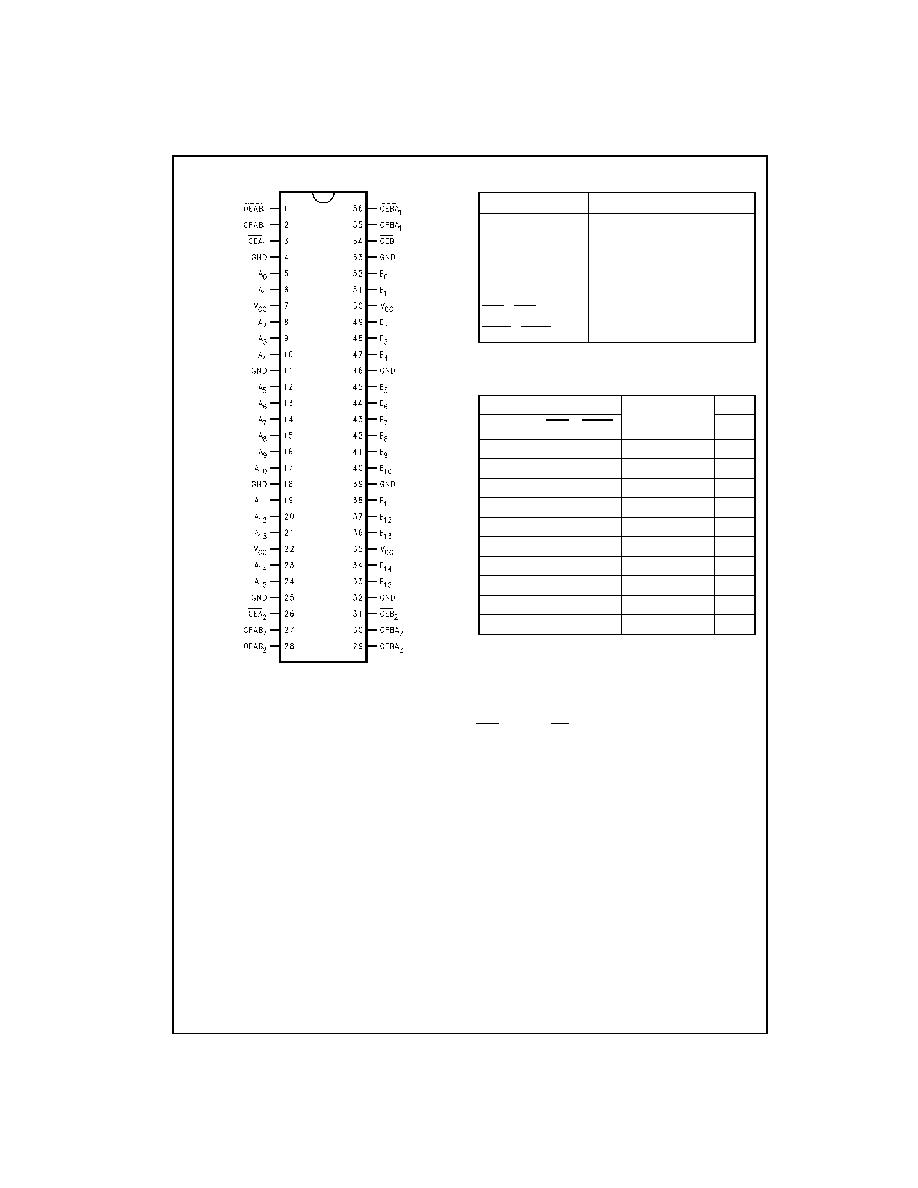
Connection Diagram
Pin Descriptions
Truth Table
(Note 1)
H
=
HIGH Voltage Level
L
=
LOW Voltage Level
X
=
Immaterial
Z
=
Output High Impedance
=
LOW-to-HIGH Transition.
NC
=
No Change (state established by last valid CP)
B
0
=
State established by last valid CP
Note 1: A to B data flow shown; B to A flow control is the same, but used
OEBA
n
, CPBA
n
and CEB
n
.
Pin Names
Description
A
0
≠A
16
Data Register A Inputs
B-Register 3-STATE Outputs
B
0
≠B
16
Data Register B Inputs
A-Register 3-STATE Outputs
CPAB
n
, CPBA
n
Clock Pulse Inputs
CEA
n
, CEB
n
Clock Enable
OEAB
n
, OEBA
n
Output Enable Inputs
Inputs
Internal Register Output
A
n
CPAB
n
CEA
n
OEAB
n
Value
B
n
X
X
H
L
NC
B
0
X
X
H
H
NC
Z
L
L
L
L
L
L
L
H
L
Z
H
L
L
H
H
H
L
H
H
Z
X
L
X
L
NC
B
0
X
H
X
L
NC
B
0
X
L
X
H
NC
Z
X
H
X
H
NC
Z
3
www.fairchildsemi.com
7
4
L
V
T1
6952
∑
74L
VTH16952
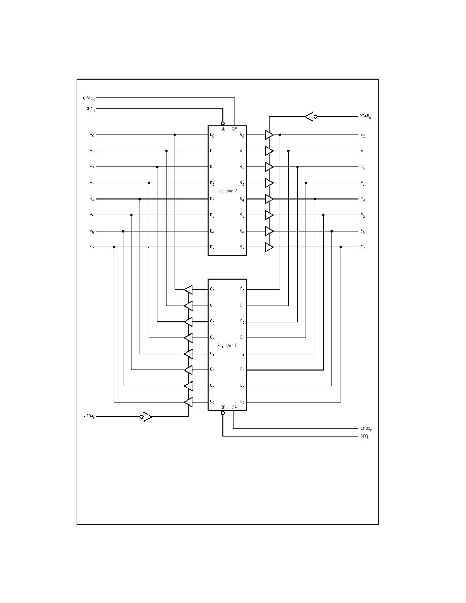
Logic Diagram
Note:
n
for either byte 1 or byte 2.
Please note that these diagrams are provided only for the understanding of logic operations and should not be used to estimate propagation delays.
www.fairchildsemi.com
4
74L
VT16952
∑
74L
VTH16952
Absolute Maximum Ratings
(Note 2)
Recommended Operating Conditions
Note 2: Absolute Maximum continuous ratings are those values beyond which damage to the device may occur. Exposure to these conditions or conditions
beyond those indicated may adversely affect device reliability. Functional operation under absolute maximum rated conditions is not implied.
Note 3: I
O
Absolute Maximum Rating must be observed.
Symbol
Parameter
Value
Conditions
Units
V
CC
Supply Voltage
-
0.5 to
+
4.6
V
V
I
DC Input Voltage
-
0.5 to
+
7.0
V
V
O
DC Output Voltage
-
0.5 to
+
7.0
Output in 3-STATE
V
-
0.5 to
+
7.0
Output in HIGH or LOW State (Note 3)
V
I
IK
DC Input Diode Current
-
50
V
I
<
GND
mA
I
OK
DC Output Diode Current
-
50
V
O
<
GND
mA
I
O
DC Output Current
64
V
O
>
V
CC
Output at HIGH State
mA
128
V
O
>
V
CC
Output at LOW State
I
CC
DC Supply Current per Supply Pin
±
64
mA
I
GND
DC Ground Current per Ground Pin
±
128
mA
T
STG
Storage Temperature
-
65 to
+
150
∞
C
Symbol
Parameter
Min
Max
Units
V
CC
Supply Voltage
2.7
3.6
V
V
I
Input Voltage
0
5.5
V
I
OH
HIGH-Level Output Current
-
32
mA
I
OL
LOW-Level Output Current
64
T
A
Free-Air Operating Temperature
-
40
+
85
∞
C
t/
V
Input Edge Rate, V
IN
=
0.8V≠2.0V, V
CC
=
3.0V
0
10
ns/V
5
www.fairchildsemi.com
7
4
L
V
T1
6952
∑
74L
VTH16952
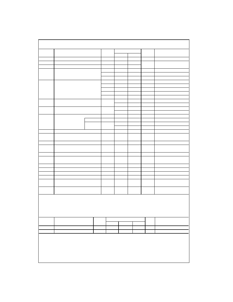
DC Electrical Characteristics
Note 4: Applies to bushold version only (74LVTH16952).
Note 5: An external driver must source at least the specified current to switch from LOW-to-HIGH.
Note 6: An external driver must sink at least the specified current to switch from HIGH-to-LOW.
Note 7: This is the increase in supply current for each input that is at the specified voltage level rather than V
CC
or GND.
Dynamic Switching Characteristics
(Note 8)
Note 8: Characterized in SSOP package. Guaranteed parameter, but not tested.
Note 9: Max number of outputs defined as (n). n
-
1 data inputs are driven 0V to 3V. Output under test held LOW.
Symbol
Parameter
V
CC
T
A
=
-
40
∞
C to
+
85
∞
C
Units
Conditions
(V)
Min
Max
V
IK
Input Clamp Diode Voltage
2.7
-
1.2
V
I
I
=
-
18 mA
V
IH
Input HIGH Voltage
2.7≠3.6
2.0
V
V
O
0.1V or
V
IL
Input LOW Voltage
2.7≠3.6
0.8
V
O
V
CC
-
0.1V
V
OH
Output HIGH Voltage
2.7≠3.6
V
CC
-
0.2
V
I
OH
=
-
100
µ
A
2.7
2.4
V
I
OH
=
-
8 mA
3.0
2.0
V
I
OH
=
-
32 mA
V
OL
Output LOW Voltage
2.7
0.2
V
I
OL
=
100
µ
A
2.7
0.5
V
I
OL
=
24 mA
3.0
0.4
V
I
OL
=
16 mA
3.0
0.5
V
I
OL
=
32 mA
3.0
0.55
V
I
OL
=
64 mA
I
I(HOLD)
Bushold Input Minimum Drive
3.0
75
µ
A
V
I
=
0.8V
(Note 4)
-
75
µ
A
V
I
=
2.0V
I
I(OD)
Bushold Input Over-Drive
3.0
500
µ
A
(Note 5)
(Note 4)
Current to Change State
-
500
µ
A
(Note 6)
I
I
Input Current
3.6
10
µ
A
V
I
=
5.5V
Control Pins
3.6
±
1
µ
A
V
I
=
0V or V
CC
Data Pins
3.6
-
5
µ
A
V
I
=
0V
1
µ
A
V
I
=
V
CC
I
OFF
Power Off Leakage Current
0
±
100
µ
A
0V
V
I
or V
O
5.5V
I
PU/PD
Power Up/Down 3-STATE
0≠1.5V
±
100
µ
A
V
O
=
0.5V to 3.0V
Output Current
V
I
=
GND or V
CC
I
OZL
3-STATE Output Leakage Current
3.6
-
5
µ
A
V
O
=
3.0V
I
OZL
3-STATE Output Leakage Current
3.6
-
5
µ
A
V
O
=
0.0V
(Note 4)
I
OZH
3-STATE Output Leakage Current
3.6
5
µ
A
V
O
=
0.5V
I
OZH
3-STATE Output Leakage Current
3.6
5
µ
A
V
O
=
3.6V
(Note 4)
I
OZH
+
3-STATE Output Leakage Current
3.6
10
µ
A
V
CC
<
V
O
5.5V
I
CCH
Power Supply Current
3.6
0.19
mA
Outputs High
I
CCL
Power Supply Current
3.6
5
mA
Outputs Low
I
CCZ
Power Supply Current
3.6
0.19
mA
Outputs Disabled
I
CCZ
+
Power Supply Current
3.6
0.19
mA
V
CC
V
O
5.5V,
Outputs Disabled
I
CC
Increase in Power Supply Current
3.6
0.2
mA
One Input at V
CC
-
0.6V
(Note 7)
Other Inputs at V
CC
or GND
Symbol
Parameter
V
CC
T
A
=
25
∞
C
Units
Conditions
(V)
Min
Typ
Max
C
L
=
50 pF, R
L
=
500
V
OLP
Quiet Output Maximum Dynamic V
OL
3.3
0.8
V
(Note 9)
V
OLV
Quiet Output Minimum Dynamic V
OL
3.3
-
0.8
V
(Note 9)