© 2005 Fairchild Semiconductor Corporation
DS012170
www.fairchildsemi.com
July 1999
Revised March 2005
7
4
L
V
T2
244 ∑ 74
L
V
TH224
4 Low V
o
lt
age Oct
a
l
Buff
er/
L
i
ne Dri
ver
w
i
t
h
3-ST
A
T
E Out
put
s and
25
:
Seri
es Resi
st
ors i
n
t
he O
u
t
put
s
74LVT2244 ∑ 74LVTH2244
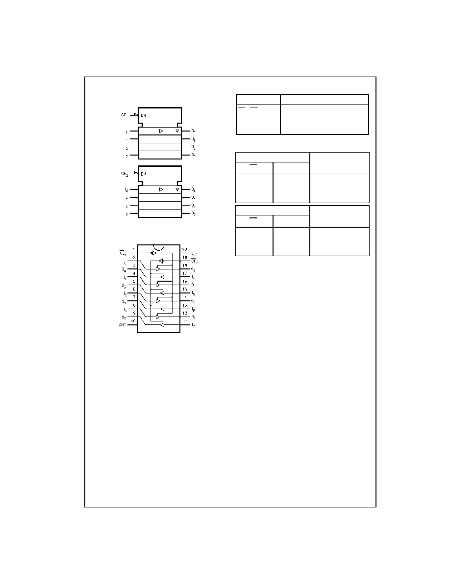
Low Voltage Octal Buffer/Line Driver
with 3-STATE Outputs
and 25
:
Series Resistors in the Outputs
General Description
The LVT2244 and LVTH2244 are octal buffers and line
drivers designed to be employed as memory address driv-
ers, clock drivers and bus oriented transmitters or receivers
which provides improved PC board density. The equivalent
25
:
-Series resistors helps reduce output overshoot and
undershoot.
The LVTH2244 data inputs include bushold, eliminating the
need for external pull-up resistors to hold unused inputs.
These octal buffers and line drivers are designed for low-
voltage (3.3V) V
CC
applications, but with the capability to
provide a TTL interface to a 5V environment. The LVT2244
and LVTH2244 are fabricated with an advanced BiCMOS
technology to achieve high speed operation similar to 5V
ABT while maintaining low power dissipation.
Features
s
Input and output interface capability to systems at
5V V
CC
s
Equivalent 25
:
-Series resistors on outputs
s
Bushold data inputs eliminate the need for external
pull-up resistors to hold unused inputs (74LVTH2244),
also available without bushold feature (74LVT2244).
s
Live insertion/extraction permitted
s
Power Up/Down high impedance provides glitch-free
bus loading
s
Outputs source/sink
12 mA/
12 mA
s
Latch-up performance exceeds 500 mA
s
ESD performance:
Human-body model
!
2000V
Machine model
!
200V
Charged-device model
!
1000V
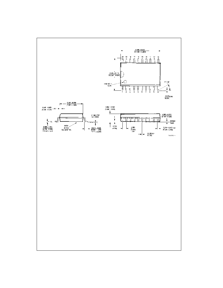
Ordering Code:
Devices also available in Tape and Reel. Specify by appending the suffix letter "X" to the ordering code.
Pb-Free package per JEDEC J-STD-020B.
Note 1: "_NL" indicates Pb-Free package (per JEDEC J-STD-020B). Device available in Tape and Reel only.
Order Number
Package
Package Description
Number
74LVT2244WM
M20B
20-Lead Small Outline Integrated Circuit (SOIC), JEDEC MS-013, 0.300" Wide
74LVT2244SJ
M20D
Pb-Free 20-Lead Small Outline Package (SOP), EIAJ TYPE II, 5.3mm Wide
74LVT2244MTC
MTC20
20-Lead Thin Shrink Small Outline Package (TSSOP), JEDEC MO-153, 4.4mm Wide
74LVT2244MTCX_NL
(Note 1)
MTC20
Pb-Free 20-Lead Thin Shrink Small Outline Package (TSSOP), JEDEC MO-153, 4.4mm
Wide
74LVTH2244WM
M20B
20-Lead Small Outline Integrated Circuit (SOIC), JEDEC MS-013, 0.300" Wide
74LVTH2244SJ
M20D
Pb-Free 20-Lead Small Outline Package (SOP), EIAJ TYPE II, 5.3mm Wide
74LVTH2244MTC
MTC20
20-Lead Thin Shrink Small Outline Package (TSSOP), JEDEC MO-153, 4.4mm Wide
74LVTH2244MTCX_NL
(Note 1)
MTC20
Pb-Free 20-Lead Thin Shrink Small Outline Package (TSSOP), JEDEC MO-153, 4.4mm
Wide

3
www.fairchildsemi.com
7
4
L
V
T2
244
∑
74L
VTH2244
Absolute Maximum Ratings
(Note 2)
Recommended Operating Conditions
Note 2: Absolute Maximum continuous ratings are those values beyond which damage to the device may occur. Exposure to these conditions or conditions
beyond those indicated may adversely affect device reliability. Functional operation under absolute maximum rated conditions is not implied.
Note 3: I
O
Absolute Maximum Rating must be observed.
DC Electrical Characteristics
Symbol
Parameter
Value
Conditions
Units
V
CC
Supply Voltage
0.5 to
4.6
V
V
I
DC Input Voltage
0.5 to
7.0
V
V
O
DC Output Voltage
0.5 to
7.0
Output in 3-STATE
V
0.5 to
7.0
Output in HIGH or LOW State (Note 3)
V
I
IK
DC Input Diode Current
50
V
I
GND
mA
I
OK
DC Output Diode Current
50
V
O
GND
mA
I
O
DC Output Current
64
V
O
!
V
CC
Output at HIGH State
mA
128
V
O
!
V
CC
Output at LOW State
I
CC
DC Supply Current per Supply Pin
r
64
mA
I
GND
DC Ground Current per Ground Pin
r
128
mA
T
STG
Storage Temperature
65 to
150
q
C
Symbol
Parameter
Min
Max
Units
V
CC
Supply Voltage
2.7
3.6
V
V
I
Input Voltage
0
5.5
V
I
OH
HIGH-Level Output Current
12
mA
I
OL
LOW-Level Output Current
12
T
A
Free-Air Operating Temperature
40
85
q
C
'
t/
'
V
Input Edge Rate, V
IN
0.8V≠2.0V, V
CC
3.0V
0
10
ns/V
Symbol
Parameter
V
CC
(V)
T
A
40
q
C to
85
q
C
Units
Conditions
Min
Typ
Max
(Note 4)
V
IK
Input Clamp Diode Voltage
2.7
1.2
V
I
I
18 mA
V
IH
Input HIGH Voltage
2.7≠3.6
2.0
V
V
O
d
0.1V or
V
IL
Input LOW Voltage
2.7≠3.6
0.8
V
O
t
V
CC
0.1V
V
OH
Output HIGH Voltage
2.7≠3.6
V
CC
0.2
V
I
OH
100
P
A
3.0
2.0
V
I
OH
12 mA
V
OL
Output LOW Voltage
2.7
0.2
V
I
OL
100
P
A
3.0
0.8
V
I
OL
12 mA
I
I(HOLD)
Bushold Input Minimum Drive
3.0
75
P
A
V
I
0.8V
(Note 5)
75
P
A
V
I
2.0V
I
I(OD)
Bushold Input Over-Drive
3.0
500
P
A
(Note 6)
(Note 5)
Current to Change State
500
P
A
(Note 7)
I
I
Input Current
3.6
10
P
A
V
I
5.5V
Control Pins
3.6
r
1
P
A
V
I
0V or V
CC
Data Pins
3.6
5
P
A
V
I
0V
1
P
A
V
I
V
CC
I
OFF
Power Off Leakage Current
0
r
100
P
A
0V
d
V
I
or V
O
d
5.5V
I
PU/PD
Power up/down 3-STATE
0≠1.5V
r
100
P
A
V
O
0.5V to 3.0V
Output Current
V
I
GND or V
CC
I
OZL
3-STATE Output Leakage Current
3.6
5
P
A
V
O
0.5V
I
OZH
3-STATE Output Leakage Current
3.6
5
P
A
V
O
3.0V
I
OZH
3-STATE Output Leakage Current
3.6
10
P
A
V
CC
V
O
d
5.5V
I
CCH
Power Supply Current
3.6
0.19
mA
Outputs HIGH
I
CCL
Power Supply Current
3.6
5
mA
Outputs LOW
I
CCZ
Power Supply Current
3.6
0.19
mA
Outputs Disabled
www.fairchildsemi.com
4
74L
VT2244
∑
74L
VTH2244
DC Electrical Characteristics
(Continued)
Note 4: All typical values are at V
CC
3.3V, T
A
25
q
C.
Note 5: Applies to bushold versions only (74LVTH2244).
Note 6: An external driver must source at least the specified current to switch from LOW-to-HIGH.
Note 7: An external driver must sink at least the specified current to switch from HIGH-to-LOW.
Note 8: This is the increase in supply current for each, input that is at the specified voltage level rather than V
CC
or GND.
Dynamic Switching Characteristics
(Note 9)
Note 9: Characterized in SOIC package. Guaranteed parameter, but not tested.
Note 10: Max number of outputs defined as (n). n
1 data inputs are driven 0V to 3V. Output under test held LOW.
AC Electrical Characteristics
Note 11: All typical values are at V
CC
3.3V, T
A
25
q
C.
Note 12: Skew is defined as the absolute value of the difference between the actual propagation delay for any two separate outputs of the same device. The
specification applies to any outputs switching in the same direction, either HIGH-to-LOW (t
OSHL
) or LOW-to-HIGH (t
OSLH
).
Capacitance
(Note 13)
Note 13: Capacitance is measured at frequency f
1 MHz, per MIL-STD-883B, Method 3012.
Symbol
Parameter
V
CC
(V)
T
A
40
q
C to
85
q
C
Units
Conditions
Min
Typ
Max
(Note 4)
I
CCZ
Power Supply Current
3.6
0.19
mA
V
CC
d
V
O
d
5.5V,
Outputs Disabled
'
I
CC
Increase in Power Supply Current
3.6
0.2
mA
One Input at V
CC
0.6V
(Note 8)
Other Inputs at V
CC
or GND
Symbol
Parameter
V
CC
T
A
25
q
C
Units
Conditions
(V)
Min
Typ
Max
C
L
50 pF, R
L
500
:
V
OLP
Quiet Output Maximum Dynamic V
OL
3.3
0.8
V
(Note 10)
V
OLV
Quiet Output Minimum Dynamic V
OL
3.3
0.8
V
Symbol
Parameter
T
A
40
q
C to
85
q
C
Units
C
L
50 pF, R
L
500
:
V
CC
3.3V
r
0.3V
V
CC
2.7V
Min
Typ
Max
Min
Max
(Note 11)
t
PLH
Propagation Delay Data to Output
1.0
4.4
1.0
5.3
ns
t
PHL
1.0
4.1
1.0
4.4
t
PZH
Output Enable Time
1.0
5.9
1.0
7.7
ns
t
PZL
1.1
5.5
1.1
6.2
t
PHZ
Output Disable Time
1.9
6.1
1.9
6.8
ns
t
PLZ
1.8
4.5
1.8
4.5
t
OSHL
Output to Output Skew
1.0
1.0
ns
t
OSLH
(Note 12)
Symbol
Parameter
Conditions
Typical
Units
C
IN
Input Capacitance
V
CC
0V, V
I
0V or V
CC
3
pF
C
OUT
Output Capacitance
V
CC
3.0V, V
O
0V or V
CC
6
pF