
© 2002 Fairchild Semiconductor Corporation
DS500433
www.fairchildsemi.com
March 2002
Revised June 2002
7
4
L
V
T3
2245
∑ 74L
VTH32245 Low
V
o
l
t
age 32-
Bit
T
r
anscei
ver wit
h
3-
ST
A
T
E Output
s
74LVT32245 ∑ 74LVTH32245
Low Voltage 32-Bit Transceiver with 3-STATE Outputs
General Description
The LVT32245 and LVTH32245 contain thirty-two non-
inverting bidirectional buffers with 3-STATE outputs and are
intended for bus oriented applications. The devices are
byte controlled. Each byte has separate control inputs
which can be shorted together for full 32-bit operation. The
T/R inputs determine the direction of data flow through the
device. The OE inputs disable both the A and B ports by
placing them in a high impedance state.
The LVTH32245 data inputs include bushold, eliminating
the need for external pull-up resistors to hold unused
inputs.
These non-inverting transceivers are designed for low volt-
age (3.3V) V
CC
applications, but with the capability to pro-
vide a TTL interface to a 5V environment. The LVT32245
and LVTH32245 are fabricated with an advanced BiCMOS
technology to achieve high speed operation similar to 5V
ABT while maintaining low power dissipation.
Features
s
Input and output interface capability to systems at
5V V
CC
s
Bushold data inputs eliminate the need for external
pull-up resistors to hold unused inputs (74LVTH32245),
also available without bushold feature (74LVT32245).
s
Live insertion/extraction permitted
s
Power Up/Down high impedance provides glitch-free
bus loading
s
Outputs source/sink
-
32 mA/
+
64 mA
s
ESD performance:
Human-body model
>
2000V
Machine model
>
200V
Charged-device model
>
1000V
s
Packaged in plastic Fine-Pitch Ball Grid Array (FBGA)
Ordering Code:
Note 1: Ordering code "G" indicates Trays.
Note 2: Devices also available in Tape and Reel. Specify by appending the suffix letter "X" to the ordering code.
Logic Symbol
Order Number
Package Number
Package Description
74LVT32245G
(Note 1)(Note 2)
BGA96A
(Preliminary)
96-Ball Fine-Pitch Ball Grid Array (FBGA), JEDEC MO-205, 5.5mm Wide
74LVTH32245G
(Note 1)(Note 2)
BGA96A
96-Ball Fine-Pitch Ball Grid Array (FBGA), JEDEC MO-205, 5.5mm Wide
www.fairchildsemi.com
2
74L
VT32245
∑
74L
VTH32245
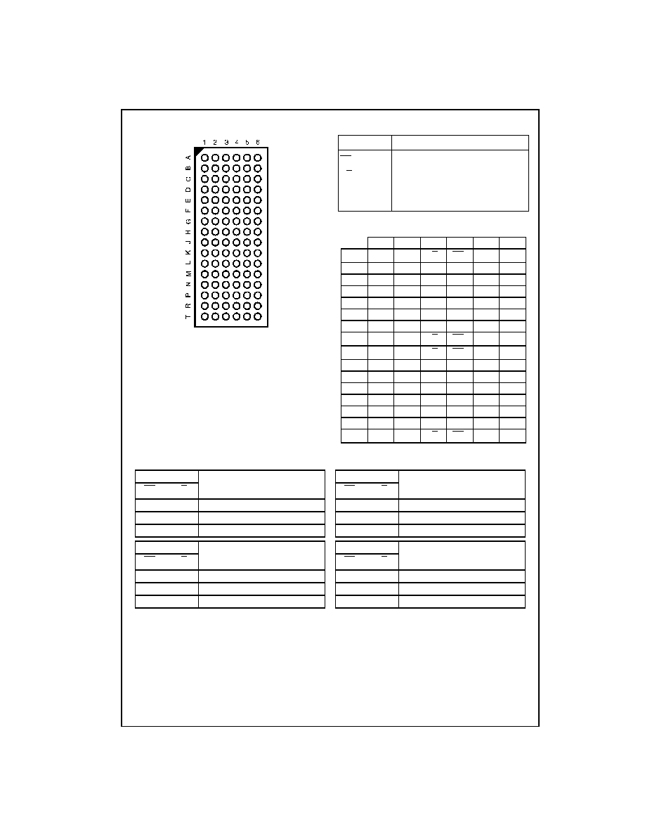
Connection Diagram
(Top Thru View)
Pin Descriptions
FBGA Pin Assignments
Truth Tables
H
=
HIGH Voltage Level
L
=
LOW Voltage Level
X
=
Immaterial
Z
=
High Impedance
Pin Names
Description
OE
n
Output Enable Input (Active LOW)
T/R
n
Transmit/Receive Input
A
0
≠A
31
Side A Inputs/3-STATE Outputs
B
0
≠B
31
Side B Inputs/3-STATE Outputs
1
2
3
4
5
6
A
B
1
B
0
T/R
1
OE
1
A
0
A
1
B
B
3
B
2
GND
GND
A
2
A
3
C
B
5
B
4
V
CC1
V
CC1
A
4
A
5
D
B
7
B
6
GND
GND
A
6
A
7
E
B
9
B
8
GND
GND
A
8
A
9
F
B
11
B
10
V
CC1
V
CC1
A
10
A
11
G
B
13
B
12
GND
GND
A
12
A
13
H
B
14
B
15
T/R
2
OE
2
A
15
A
14
J
B
17
B
16
T/R
3
OE
3
A
16
A
17
K
B
19
B
18
GND
GND
A
18
A
19
L
B
21
B
20
V
CC2
V
CC2
A
20
A
21
M
B
23
B
22
GND
GND
A
22
A
23
N
B
25
B
24
GND
GND
A
24
A
25
P
B
27
B
26
V
CC2
V
CC2
A
26
A
27
R
B
29
B
28
GND
GND
A
28
A
29
T
B
30
B
31
T/R
4
OE
4
A
31
A
30
Inputs
Outputs
Inputs
Outputs
OE
1
T/R
1
OE
3
T/R
3
L
L
Bus B
0
≠B
7
Data to Bus A
0
≠A
7
L
L
Bus B
16
≠B
23
Data to Bus A
16
≠A
23
L
H
Bus A
0
≠A
7
Data to Bus B
0
≠B
7
L
H
Bus A
16
≠A
23
Data to Bus B
16
≠B
23
H
X
HIGH≠Z State on A
0
≠A
7
,B
0
≠B
7
H
X
HIGH≠Z State on A
16
≠A
23
,B
16
≠B
23
Inputs
Outputs
Inputs
Outputs
OE
2
T/R
2
OE
4
T/R
4
L
L
Bus B
8
≠B
15
Data to Bus A
8
≠A
15
L
L
Bus B
24
≠B
31
Data to Bus A
24
≠A
31
L
H
Bus A
8
≠A
15
Data to Bus B
8
≠B
15
L
H
Bus B
24
≠A
31
Data to Bus B
24
≠B
31
H
X
HIGH≠Z State on A
8
≠A
15
,B
8
≠B
15
H
X
HIGH≠Z State on A
24
≠A
31
,B
24
≠B
31
3
www.fairchildsemi.com
7
4
L
V
T3
2245
∑
74L
VTH32245
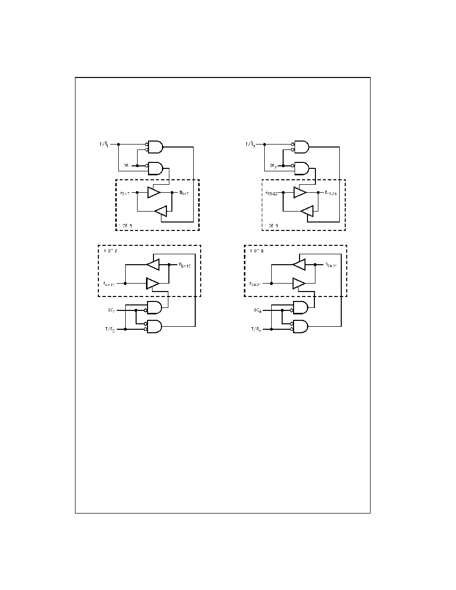
Functional Description
The LVT32245 and LVTH32245 contain thirty-two non-inverting bidirectional buffers with 3-STATE outputs. The device is
byte controlled with each byte functioning identically, but independent of the other. The control pins can be shorted together
to obtain 16-bit or full 32-bit operation.
Logic Diagrams
Byte 1
Byte 2
Byte 3
Byte 4
V
CC1
is associated with Bytes 1 and 2.
V
CC2
is associated with Bytes 3 and 4.
Note: Please note that these diagrams are provided only for the understanding of logic operations and should not be used to estimate propagation delays.
www.fairchildsemi.com
4
74L
VT32245
∑
74L
VTH32245
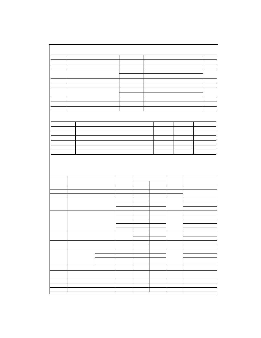
Absolute Maximum Ratings
(Note 3)
Recommended Operating Conditions
Note 3: Absolute Maximum continuous ratings are those values beyond which damage to the device may occur. Exposure to these conditions or conditions
beyond those indicated may adversely affect device reliability. Functional operation under absolute maximum rated conditions is not implied.
Note 4: I
O
Absolute Maximum Ratings must be observed.
DC Electrical Characteristics
Symbol
Parameter
Value
Conditions
Units
V
CC
Supply Voltage
-
0.5 to
+
4.6
V
V
I
DC Input Voltage
-
0.5 to
+
7.0
V
V
O
Output Voltage
-
0.5 to
+
7.0
Output in 3-STATE
V
-
0.5 to
+
7.0
Output in HIGH or LOW State (Note 4)
I
IK
DC Input Diode Current
-
50
V
I
<
GND
mA
I
OK
DC Output Diode Current
-
50
V
O
<
GND
mA
I
O
DC Output Current
64
Output at HIGH State, V
O
>
V
CC
mA
128
Output at LOW State, V
O
>
V
CC
I
CC
DC Supply Current per Supply Pin
±
64
mA
I
GND
DC Ground Current per Ground Pin
±
128
mA
T
STG
Storage Temperature Range
-
65 to
+
150
∞
C
Symbol
Parameter
Min
Max
Units
V
CC
Supply Voltage
2.7
3.6
V
V
I
Input Voltage
0
5.5
V
I
OH
HIGH-Level Output Current
-
32
mA
I
OL
LOW-Level Output Current
64
mA
T
A
Free-Air Operating Temperature
-
40
+
85
∞
C
t/
V
Input Edge Rate, V
IN
=
0.8V≠2.0V, V
CC
=
3.0V
0
10
ns/V
Symbol
Parameter
V
CC
T
A
=
-
40
∞
C to
+
85
∞
C
Units
Conditions
(V)
Min
Max
V
IK
Input Clamp Diode Voltage
2.7
-
1.2
V
I
I
=
-
18 mA
V
IH
Input HIGH Voltage
2.7≠3.6
2.0
V
V
O
0.1V or
V
IL
Input LOW Voltage
2.7≠3.6
0.8
V
V
O
V
CC
-
0.1V
V
OH
Output HIGH Voltage
2.7≠3.6
V
CC
-
0.2
V
I
OH
=
-
100
µ
A
2.7
2.4
I
OH
=
-
8 mA
3.0
2.0
I
OH
=
-
32 mA
V
OL
Output LOW Voltage
2.7
0.2
V
I
OL
=
100
µ
A
2.7
0.5
I
OL
=
24 mA
3.0
0.4
I
OL
=
16 mA
3.0
0.5
I
OL
=
32 mA
3.0
0.55
I
OL
=
64 mA
I
I(HOLD)
Bushold Input Minimum Drive
3.0
75
µ
A
V
I
=
0.8V
(Note 5)
-
75
V
I
=
2.0V
I
I(OD)
Bushold Input Over-Drive
3.0
500
µ
A
(Note 6)
(Note 5)
Current to Change State
-
500
(Note 7)
I
I
Input Current
3.6
10
µ
A
V
I
=
5.5V
Control Pins
3.6
±
1
V
I
=
0V or V
CC
Data Pins
3.6
-
5
V
I
=
0V
1
V
I
=
V
CC
I
OFF
Power Off Leakage Current
0
±
100
µ
A
0V
V
I
or V
O
5.5V
I
PU/PD
Power Up/Down 3-STATE
0≠1.5
±
100
µ
A
V
O
=
0.5V to 3.0V
Output Current
V
I
=
GND or V
CC
I
OZL
3-STATE Output Leakage Current
3.6
-
5
µ
A
V
O
=
0.5V
I
OZL
(Note 5)
3-STATE Output Leakage Current
3.6
-
5
µ
A
V
O
=
0.0V
I
OZH
3-STATE Output Leakage Current
3.6
5
µ
A
V
O
=
3.0V
5
www.fairchildsemi.com
7
4
L
V
T3
2245
∑
74L
VTH32245
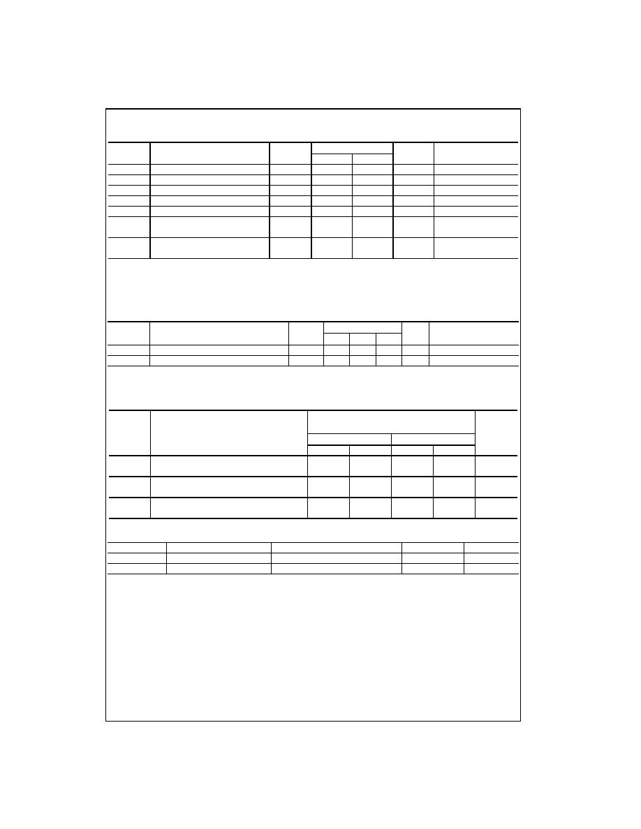
DC Electrical Characteristics
(Continued)
Note 5: Applies to bushold versions only (74LVTH32245).
Note 6: An external driver must source at least the specified current to switch from LOW-to-HIGH.
Note 7: An external driver must sink at least the specified current to switch from HIGH-to-LOW.
Note 8: This is the increase in supply current for each input that is at the specified voltage level rather than V
CC
or GND.
Dynamic Switching Characteristics
(Note 9)
Note 9: Characterized in SSOP package. Guaranteed parameter, but not tested.
Note 10: Max number of outputs defined as (n). n
-
1 data inputs are driven 0V to 3V. Output under test held LOW.
AC Electrical Characteristics
Capacitance
(Note 11)
Note 11: Capacitance is measured at frequency f
=
1 MHz, per MIL-STD-883, Method 3012.
Symbol
Parameter
V
CC
T
A
=
-
40
∞
C to
+
85
∞
C
Units
Conditions
(V)
Min
Max
I
OZH
(Note 5) 3-STATE Output Leakage Current
3.6
5
µ
A
V
O
=
3.6V
I
OZH
+
3-STATE Output Leakage Current
3.6
10
µ
A
V
CC
<
V
O
5.5V
I
CCH
Power Supply Current
V
CC1
or V
CC2
3.6
0.19
mA
Outputs HIGH
I
CCL
Power Supply Current
V
CC1
or V
CC2
3.6
5.0
mA
Outputs LOW
I
CCZ
Power Supply Current
V
CC1
or V
CC2
3.6
0.19
mA
Outputs Disabled
I
CCZ
+
Power Supply Current
V
CC1
or V
CC2
3.6
0.19
mA
V
CC
V
O
5.5V,
Outputs Disabled
I
CC
Increase in Power Supply Current
3.6
0.2
mA
One Input at V
CC
-
0.6V
(Note 8)
V
CC1
or V
CC2
Other Inputs at V
CC
or GND
Symbol
Parameter
V
CC
T
A
=
25
∞
C
Units
Conditions
(V)
Min
Typ
Max
C
L
=
50 pF, R
L
=
500
V
OLP
Quiet Output Maximum Dynamic V
OL
3.3
0.8
V
(Note 10)
V
OLV
Quiet Output Minimum Dynamic V
OL
3.3
-
0.8
V
(Note 10)
Symbol
Parameter
T
A
=
-
40
∞
C to
+
85
∞
C
Units
C
L
=
50 pF, R
L
=
500
V
CC
=
3.3V
±
0.3V
V
CC
=
2.7V
Min
Max
Min
Max
t
PLH
Propagation Delay Data to Output
1.5
3.5
1.5
3.9
ns
t
PHL
1.3
3.5
1.3
3.9
t
PZH
Output Enable Time
1.5
4.5
1.5
5.3
ns
t
PZL
1.6
5.3
1.6
6.9
t
PHZ
Output Disable Time
2.3
5.4
2.3
6.1
ns
t
PLZ
2.2
5.1
2.2
5.4
Symbol
Parameter
Conditions
Typical
Units
C
IN
Input Capacitance
V
CC
=
0V, V
I
=
0V or V
CC
4
pF
C
I/O
Input/Output Capacitance
V
CC
=
3.0V, V
O
=
0V or V
CC
8
pF