Preliminary
© 2001 Fairchild Semiconductor Corporation
DS500548
www.fairchildsemi.com
August 2001
Revised August 2001
7
4
L
V
T3
2373
∑ 74L
VTH32373 Low
V
o
l
t
age 32-
Bit
T
r
anspare
n
t Latch wit
h
3
-
ST
A
T
E
Output
s (Pre
li
m
i
nary)
74LVT32373 ∑ 74LVTH32373
Low Voltage 32-Bit Transparent Latch
with 3-STATE Outputs (Preliminary)
General Description
The LVT32373 and LVTH32373 contain thirty-two non-
inverting latches with 3-STATE outputs and are intended
for bus oriented applications. The device is byte controlled.
The flip-flops appear transparent to the data when the
Latch Enable (LE) is HIGH. When LE is LOW, the data that
meets the setup time is latched. Data appears on the bus
when the Output Enable (OE) is LOW. When OE is HIGH,
the outputs are in a high impedance state.
The LVTH32373 data inputs include bushold, eliminating
the need for external pull-up resistors to hold unused
inputs.
These latches are designed for low-voltage (3.3V) V
CC
applications, but with the capability to provide a TTL inter-
face to a 5V environment. The LVT32373 and LVTH32373
are fabricated with an advanced BiCMOS technology to
achieve high speed operation similar to 5V ABT while
maintaining a low power dissipation.
Features
s
Input and output interface capability to systems at
5V V
CC
s
Bushold data inputs eliminate the need for external
pull-up resistors to hold unused inputs (74LVTH32373),
also available without bushold feature (74LVT32373)
s
Live insertion/extraction permitted
s
Power Up/Down high impedance provides glitch-free
bus loading
s
Outputs source/sink
-
32 mA/
+
64 mA
s
ESD performance:
Human-body model
>
2000V
Machine model
>
200V
Charged-device model
>
1000V
s
Packaged in plastic Fine-Pitch Ball Grid Array (FBGA)
(Preliminary)
Ordering Code:
Note 1: BGA package available in Tape and Reel only.
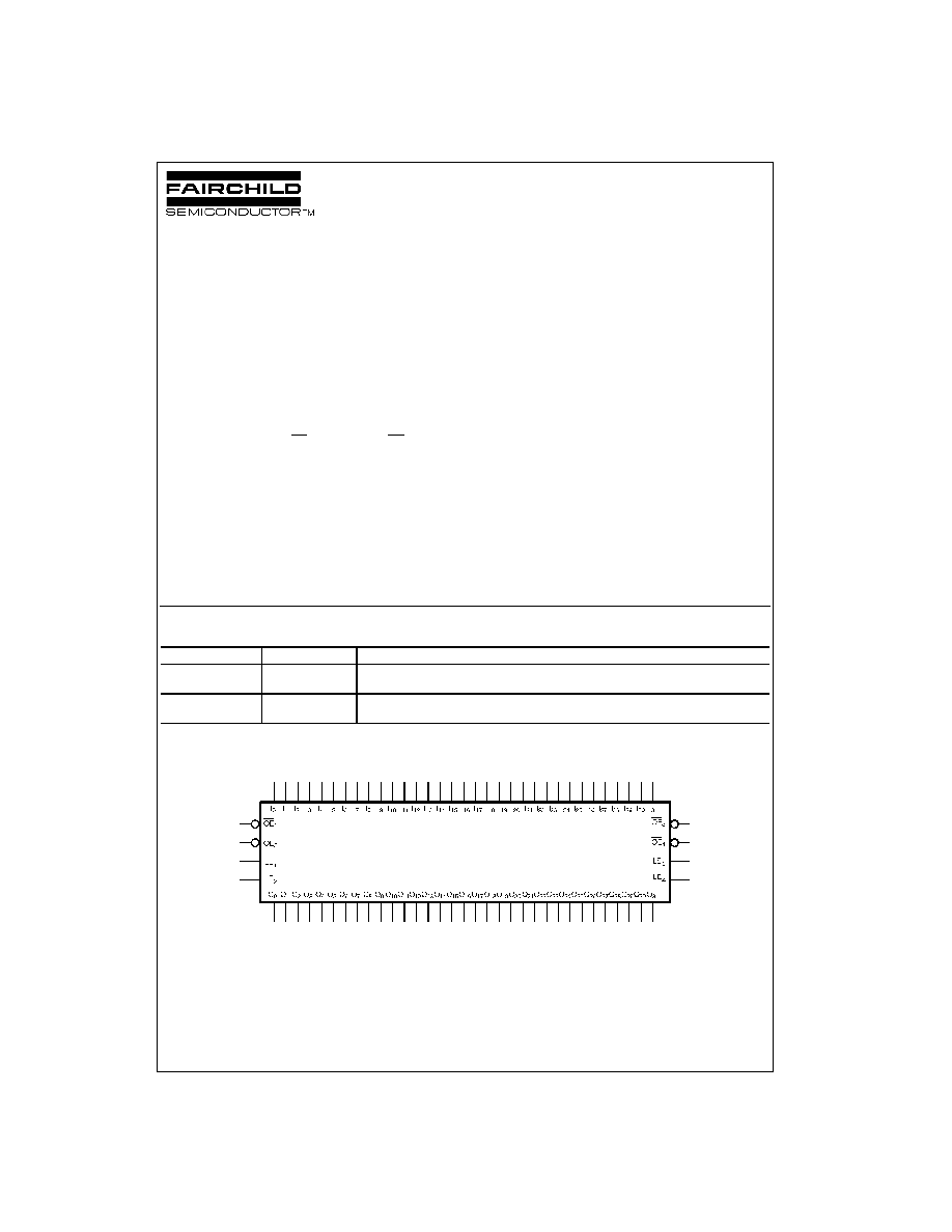
Logic Symbol
Order Number
Package Number
Package Description
74LVT32373GX
(Note 1)
BGA96A
(Preliminary)
96-Ball Fine-Pitch Ball Grid Array (FBGA), JEDEC MO-205, 5.5mm Wide
[TAPE and REEL]
74LVTH32373GX
(Note 1)
BGA96A
(Preliminary)
96-Ball Fine-Pitch Ball Grid Array (FBGA), JEDEC MO-205, 5.5mm Wide
[TAPE and REEL]
Preliminary
www.fairchildsemi.com
2
74L
VT32373
∑
74L
VTH32373
Connection Diagram
(Top Thru View)
Pin Descriptions
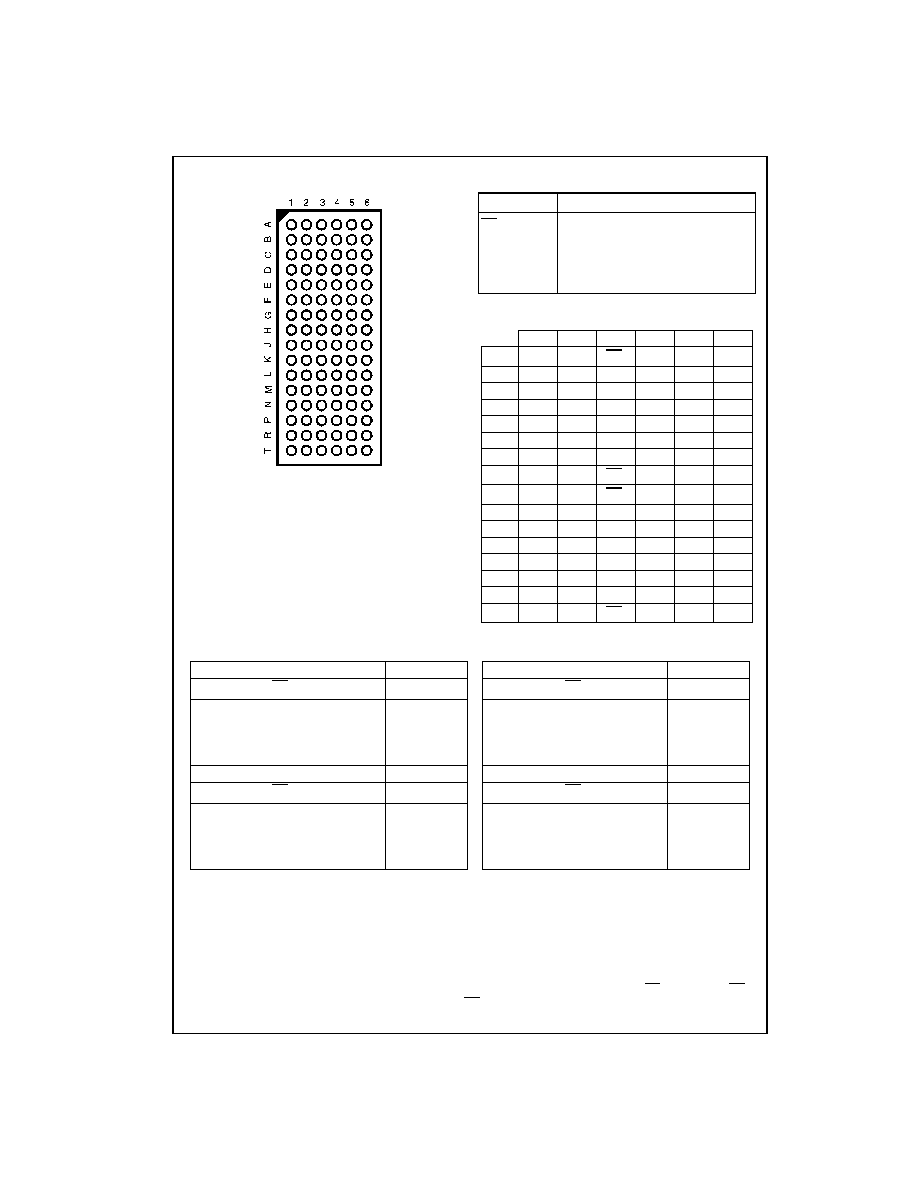
FBGA Pin Assignments
Truth Table
H
=
HIGH Voltage Level
L
=
LOW Voltage Level
X
=
Immaterial
Z
=
HIGH Impedance
O
o
=
Previous O
o
prior to HIGH-to-LOW transition of LE
Functional Description
The LVT32373 and LVTH32373 contain thirty-two D-type latches with 3-STATE standard outputs. The device is byte con-
trolled with each byte functioning identically, but independent of the other. Control pins can be shorted together to obtain full
32-bit operation. The following description applies to each byte. When the Latch Enable (LE
n
) input is HIGH, data on the D
n
enters the latches. In this condition the latches are transparent, i.e, a latch output will change states each time its D input
changes. When LE
n
is LOW, the latches store information that was present on the D inputs a setup time preceding the
HIGH-to-LOW transition of LE
n
. The 3-STATE standard outputs are controlled by the Output Enable (OE
n
) input. When OE
n
is LOW, the standard outputs are in the 2-state mode. When OE
n
is HIGH, the standard outputs are in the high impedance
mode but this does not interfere with entering new data into the latches.
Pin Names
Description
OE
n
Output Enable Input (Active LOW)
LE
n
Latch Enable Input
I
0
≠I
31
Inputs
O
0
≠O
31
3-STATE Outputs
1
2
3
4
5
6
A
O
1
O
0
OE
1
LE
1
I
0
I
1
B
O
3
O
2
GND
GND
I
2
I
3
C
O
5
O
4
V
CC1
V
CC1
I
4
I
5
D
O
7
O
6
GND
GND
I
6
I
7
E
O
9
O
8
GND
GND
I
8
I
9
F
O
11
O
10
V
CC1
V
CC1
I
10
I
11
G
O
13
O
12
GND
GND
I
12
I
13
H
O
14
O
15
OE
2
LE
2
I
15
I
14
J
O
17
O
16
OE
3
LE
3
I
16
I
17
K
O
19
O
18
GND
GND
I
18
I
19
L
O
21
O
20
V
CC2
V
CC2
I
20
I
21
M
O
23
O
22
GND
GND
I
22
I
23
N
O
25
O
24
GND
GND
I
24
I
25
P
O
27
O
26
V
CC2
V
CC2
I
26
I
27
R
O
29
O
28
GND
GND
I
28
I
29
T
O
30
O
31
OE
4
LE
4
I
31
I
30
Inputs
Outputs
Inputs
Outputs
CP
1
OE
1
I
0
≠I
7
O
0
≠O
7
CP
2
OE
2
I
8
≠I
15
O
8
≠O
15
X
H
X
Z
X
H
X
Z
H
L
L
L
H
L
L
L
H
L
H
H
H
L
H
H
L
L
X
O
0
L
L
X
O
0
Inputs
Outputs
Inputs
Outputs
CP
3
OE
3
I
16
≠I
23
O
16
≠O
23
CP
4
OE
4
I
24
≠I
31
O
24
≠O
31
X
H
X
Z
X
H
X
Z
H
L
L
L
H
L
L
L
H
L
H
H
H
L
H
H
L
L
X
O
0
L
L
X
O
0

Preliminary
3
www.fairchildsemi.com
7
4
L
V
T3
2373
∑
74L
VTH32373
Logic Diagrams
Byte 1 (0:7)
Byte 2 (8:15)
Byte 3 (16:23)
Byte 4 (24:31)
V
CC1
is associated with Bytes 1 and 2.
V
CC2
is associated with Bytes 3 and 4.
Note: Please note that these diagrams are provided only for the understanding of logic operations and should not be used to estimate propagation delays.
Preliminary
www.fairchildsemi.com
4
74L
VT32373
∑
74L
VTH32373
Absolute Maximum Ratings
(Note 2)
Recommended Operating Conditions
Note 2: Absolute Maximum continuous ratings are those values beyond which damage to the device may occur. Exposure to these conditions or conditions
beyond those indicated may adversely affect device reliability. Functional operation under absolute maximum rated conditions is not implied.
Note 3: I
O
Absolute Maximum Rating must be observed.
DC Electrical Characteristics
Symbol
Parameter
Value
Conditions
Units
V
CC
Supply Voltage
-
0.5 to
+
4.6
V
V
I
DC Input Voltage
-
0.5 to
+
7.0
V
V
O
DC Output Voltage
-
0.5 to
+
7.0
Output in 3-STATE
V
-
0.5 to
+
7.0
Output in HIGH or LOW State (Note 3)
I
IK
DC Input Diode Current
-
50
V
I
<
GND
mA
I
OK
DC Output Diode Current
-
50
V
O
<
GND
mA
I
O
DC Output Current
64
V
O
>
V
CC
Output at HIGH State
mA
128
V
O
>
V
CC
Output at LOW State
I
CC
DC Supply Current per Supply Pin
±
64
mA
I
GND
DC Ground Current per Ground Pin
±
128
mA
T
STG
Storage Temperature
-
65 to
+
150
∞
C
Symbol
Parameter
Min
Max
Units
V
CC
Supply Voltage
2.7
3.6
V
V
I
Input Voltage
0
5.5
V
I
OH
HIGH Level Output Current
-
32
mA
I
OL
LOW Level Output Current
64
mA
T
A
Free-Air Operating Temperature
-
40
85
∞
C
t/
V
Input Edge Rate, V
IN
=
0.8V≠2.0V, V
CC
=
3.0V
0
10
ns/V
Symbol
Parameter
V
CC
T
A
=
-
40
∞
C to
+
85
∞
C
Units
Conditions
(V)
Min
Max
V
IK
Input Clamp Diode Voltage
2.7
-
1.2
V
I
I
=
-
18 mA
V
IH
Input HIGH Voltage
2.7≠3.6
2.0
V
V
O
0.1V or
V
IL
Input LOW Voltage
2.7≠3.6
0.8
V
V
O
V
CC
-
0.1V
V
OH
Output HIGH Voltage
2.7≠3.6
V
CC
-
0.2
V
I
OH
=
-
100
µ
A
2.7
2.4
I
OH
=
-
8 mA
3.0
2.0
I
OH
=
-
32 mA
V
OL
Output LOW Voltage
2.7
0.2
V
I
OL
=
100
µ
A
2.7
0.5
I
OL
=
24 mA
3.0
0.4
I
OL
=
16 mA
3.0
0.5
I
OL
=
32 mA
3.0
0.55
I
OL
=
64 mA
I
I(HOLD)
Bushold Input Minimum Drive
3.0
75
µ
A
V
I
=
0.8V
(Note 4)
-
75
V
I
=
2.0V
I
I(OD)
Bushold Input Over-Drive
3.0
500
µ
A
(Note 5)
(Note 4)
Current to Change State
-
500
(Note 6)
I
I
Input Current
3.6
10
µ
A
V
I
=
5.5V
Control Pins
3.6
±
1
V
I
=
0V or V
CC
Data Pins
3.6
-
5
V
I
=
0V
1
V
I
=
V
CC
I
OFF
Power Off Leakage Current
0
±
100
µ
A
0V
V
I
or V
O
5.5V
I
PU/PD
Power up/down 3-STATE
0≠1.5V
±
100
µ
A
V
O
=
0.5V to 3.0V
Output Current
V
I
=
GND or V
CC
I
OZL
3-STATE Output Leakage Current
3.6
-
5
µ
A
V
O
=
0.5V
I
OZH
3-STATE Output Leakage Current
3.6
5
µ
A
V
O
=
3.0V
I
OZH
+
3-STATE Output Leakage Current
3.6
10
µ
A
V
CC
<
V
O
5.5V

Preliminary
5
www.fairchildsemi.com
7
4
L
V
T3
2373
∑
74L
VTH32373
DC Electrical Characteristics
(Continued)
Note 4: Applies to bushold versions only (74LVTH32373).
Note 5: An external driver must source at least the specified current to switch from LOW-to-HIGH.
Note 6: An external driver must sink at least the specified current to switch from HIGH-to-LOW.
Note 7: This is the increase in supply current for each input that is at the specified voltage level rather than V
CC
or GND.
Dynamic Switching Characteristics
(Note 8)
Note 8: Characterized in SSOP package. Guaranteed parameter, but not tested.
Note 9: Max number of outputs defined as (n). n
-
1 data inputs are driven 0V to 3V. Output under test held LOW.
AC Electrical Characteristics
Capacitance
(Note 10)
Note 10: Capacitance is measured at frequency f
=
1 MHz, per MIL-STD-883, Method 3012.
Symbol
Parameter
V
CC
T
A
=
-
40
∞
C to
+
85
∞
C
Units
Conditions
(V)
Min
Max
I
CCH
Power Supply Current
(V
CC1
or V
CC2
)
3.6
0.19
mA
Outputs HIGH
I
CCL
Power Supply Current
(V
CC1
or V
CC2
)
3.6
5
mA
Outputs LOW
I
CCZ
Power Supply Current
(V
CC1
or V
CC2
)
3.6
0.19
mA
Outputs Disabled
I
CCZ
+
Power Supply Current
(V
CC1
or V
CC2
)
3.6
0.19
mA
V
CC
V
O
5.5V,
Outputs Disabled
I
CC
Increase in Power Supply Current
(V
CC1
or V
CC2
)
3.6
0.2
mA
One Input at V
CC
-
0.6V
(Note 7)
Other Inputs at V
CC
or GND
Symbol
Parameter
V
CC
T
A
=
25
∞
C
Units
Conditions
(V)
Min
Typ
Max
C
L
=
50 pF, R
L
=
500
V
OLP
Quiet Output Maximum Dynamic V
OL
3.3
0.8
V
(Note 9)
V
OLV
Quiet Output Minimum Dynamic V
OL
3.3
-
0.8
V
(Note 9)
Symbol
Parameter
T
A
=
-
40
∞
C to
+
85
∞
C, C
L
=
50pF, R
L
=
500
Units
V
CC
=
3.3V
±
0.3V
V
CC
=
2.7V
Min
Max
Min
Max
t
PHL
Propagation Delay
1.5
3.9
1.5
4.3
ns
t
PLH
D
n
to O
n
1.5
3.8
1.5
4.2
t
PHL
Propagation Delay
1.9
4.2
1.9
4.4
ns
t
PLH
LE to O
n
1.6
4.3
1.6
4.8
t
PZL
Output Enable Time
1.3
4.3
1.3
4.9
ns
t
PZH
1.0
4.3
1.0
5.1
t
PLZ
Output Disable Time
1.5
4.7
1.5
4.8
ns
t
PHZ
2.0
5.0
2.0
5.4
t
S
Setup Time, D
n
to LE
1.0
0.8
ns
t
H
Hold Time, D
n
to LE
1.0
1.1
ns
t
W
LE Pulse Width
3.0
3.0
ns
Symbol
Parameter
Conditions
Typical
Units
C
IN
Input Capacitance
V
CC
=
Open, V
I
=
0V or V
CC
4
pF
C
OUT
Output Capacitance
V
CC
=
3.0V, V
O
=
0V or V
CC
8
pF
Preliminary
www.fairchildsemi.com
6
74L
VT32373
∑
74L
VTH
3
2373 Low
V
o
lt
age 32-Bi
t T
r
ans
parent
Lat
ch w
i
th
3-
ST
A
T
E O
u
t
put
s
(
P
rel
i
mina
ry)
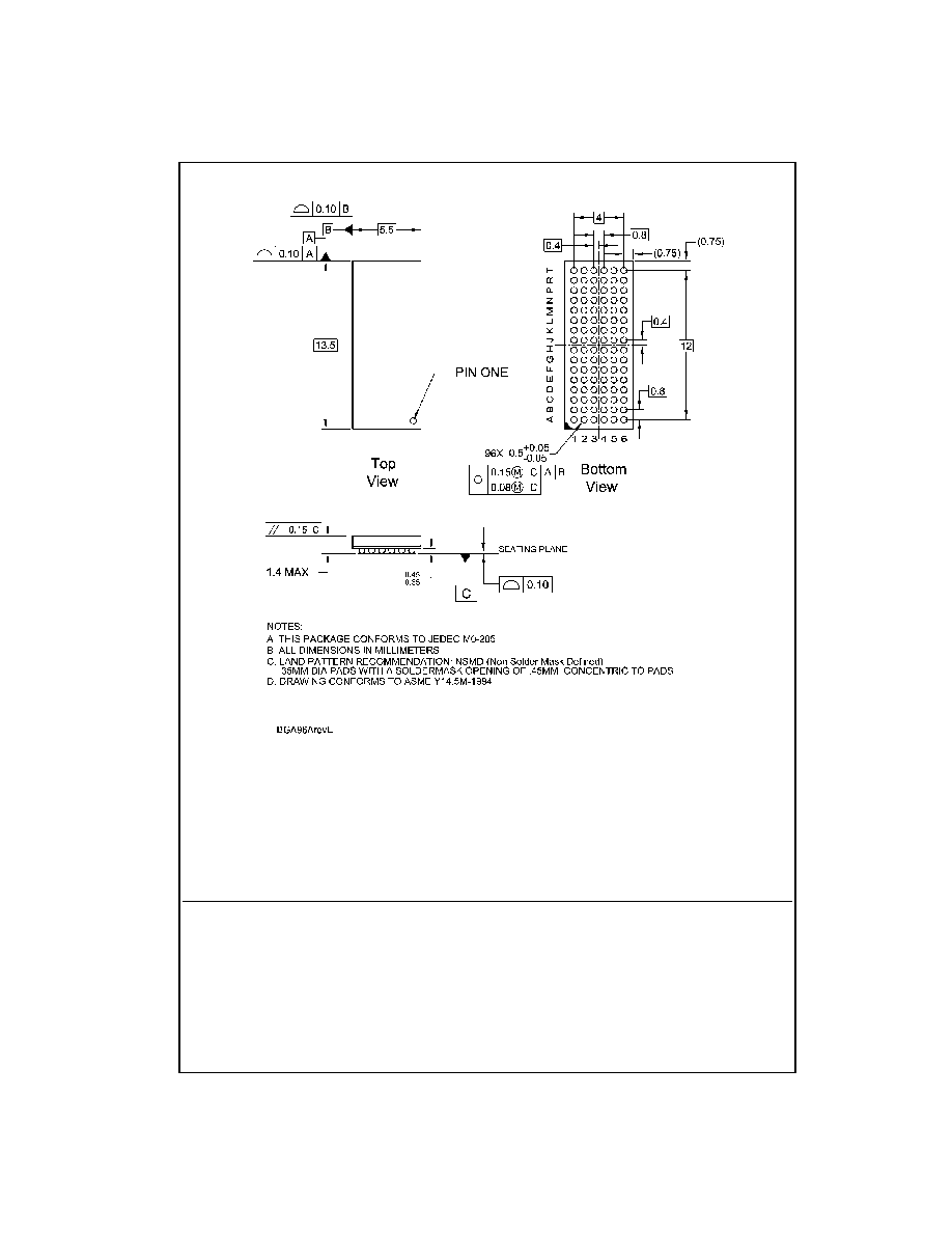
Physical Dimensions
inches (millimeters) unless otherwise noted
96-Ball Fine-Pitch Ball Grid Array (FBGA), JEDEC MO-205, 5.5mm Wide
Package Number BGA96A
Preliminary
Fairchild does not assume any responsibility for use of any circuitry described, no circuit patent licenses are implied and
Fairchild reserves the right at any time without notice to change said circuitry and specifications.
LIFE SUPPORT POLICY
FAIRCHILD'S PRODUCTS ARE NOT AUTHORIZED FOR USE AS CRITICAL COMPONENTS IN LIFE SUPPORT
DEVICES OR SYSTEMS WITHOUT THE EXPRESS WRITTEN APPROVAL OF THE PRESIDENT OF FAIRCHILD
SEMICONDUCTOR CORPORATION. As used herein:
1. Life support devices or systems are devices or systems
which, (a) are intended for surgical implant into the
body, or (b) support or sustain life, and (c) whose failure
to perform when properly used in accordance with
instructions for use provided in the labeling, can be rea-
sonably expected to result in a significant injury to the
user.
2. A critical component in any component of a life support
device or system whose failure to perform can be rea-
sonably expected to cause the failure of the life support
device or system, or to affect its safety or effectiveness.
www.fairchildsemi.com