© 2000 Fairchild Semiconductor Corporation
DS012448
www.fairchildsemi.com
April 2000
Revised April 2000
7
4
L
V
TH54
3 Low
V
o
l
t
a
ge Oct
a
l
Regist
ere
d
T
r
anscei
ver
wit
h
3-
ST
A
T
E
Output
s
74LVTH543
Low Voltage Octal Registered Transceiver
with 3-STATE Outputs
General Description
The LVTH543 octal transceiver contains two sets of D-type
latches for temporary storage of data flowing in either
direction. Separate Latch Enable and Output Enable inputs
are provided for each register to permit independent con-
trol of inputting and outputting in either direction of data
flow.
The LVTH543 data inputs include bushold, eliminating the
need for external pull-up resistors to hold unused inputs.
This octal registered transceiver is designed for low-volt-
age (3.3V) V
CC
applications, but with the capability to pro-
vide a TTL interface to a 5V environment. The LVTH543 is
fabricated with an advanced BiCMOS technology to
achieve high speed operation similar to 5V ABT while
maintaining a low power dissipation.
Features
s
Input and output interface capability to systems at
5V V
CC
s
Bushold data inputs eliminate the need for external pull-
up resistors to hold unused inputs
s
Live insertion/extraction permitted
s
Power Up/Down high impedance provides glitch-free
bus loading
s
Outputs source/sink
-
32 mA/
+
64 mA
s
Functionally compatible with the 74 series 543
s
Latch-up performance exceeds 500 mA
Ordering Code:
Device also available in Tape and Reel. Specify by appending suffix letter "X" to the ordering code.
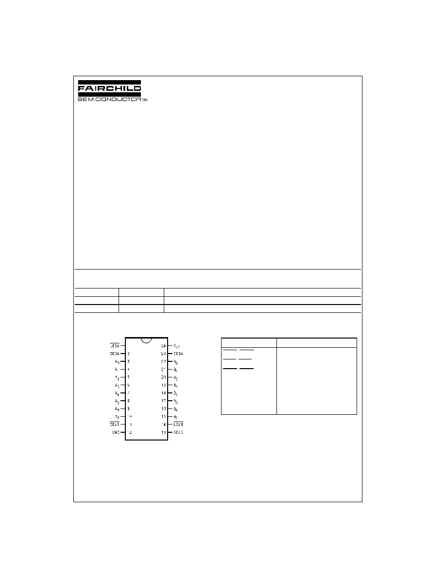
Connection Diagram
Pin Descriptions
Order Number
Package Number
Package Description
74LVTH543WM
M24B
24-Lead Small Outline Integrated Circuit (SOIC), JEDEC MS-013, 0.300" Wide
74LVTH543MTC
MTC24
24-Lead Thin Shrink Small Outline Package (TSSOP), JEDEC MO-153, 4.4mm Wide
Pin Names
Description
OEAB, OEBA
Output Enable Inputs
LEAB, LEBA
Latch Enable Inputs
CEAB, CEBA
Chip Enable Inputs
A
0
≠A
7
Side A Inputs or
3-STATE Outputs
B
0
≠B
7
Side B Inputs or
3-STATE Outputs

www.fairchildsemi.com
2
74
L
V
TH543
Logic Symbols
IEEE/IEC
Functional Description
The LVTH543 contains two sets of D-type latches, with
separate input and output controls for each. For data flow
from A to B, for example, the A to B Enable (CEAB) input
must be LOW in order to enter data from the A Port or take
data from the B Port as indicated in the Data I/O Control
Table. With CEAB LOW, a low signal on (LEAB) input
makes the A to B latches transparent; a subsequent LOW-
to-HIGH transition of the LEAB line puts the A latches in
the storage mode and their outputs no longer change with
the A inputs. With CEAB and OEAB both LOW, the B out-
put buffers are active and reflect the data present on the
output of the A latches. Control of data flow from B to A is
similar, but using the CEBA, LEBA and OEBA.
Data I/O Control Table
H
=
HIGH Voltage Level
L
=
LOW Voltage Level
X
=
Immaterial
Note: A-to-B data flow shown; B-to-A flow control is the same, except
using CEBA, LEBA, and OEBA.
Logic Diagram
Please not that this diagram is provided only for the understanding of logic operations and should not be used to estimate propagation delays.
Inputs
Latch Status
Output
CEAB
LEAB
OEAB
Buffers
H
X
X
Latched
High Z
X
H
X
Latched
--
L
L
X
Transparent
--
X
X
H
--
High Z
L
X
L
--
Driving

3
www.fairchildsemi.com
7
4
L
V
TH54
3
Absolute Maximum Ratings
(Note 1)
Recommended Operating Conditions
Note 1: Absolute Maximum continuous ratings are those values beyond which damage to the device may occur. Exposure to these conditions or conditions
beyond those indicated may adversely affect device reliability. Functional operation under absolute maximum rated conditions is not implied.
Note 2: I
O
Absolute Maximum Rating must be observed.
Symbol
Parameter
Value
Conditions
Units
V
CC
Supply Voltage
-
0.5 to
+
4.6
V
V
I
DC Input Voltage
-
0.5 to
+
7.0
V
V
O
DC Output Voltage
-
0.5 to
+
7.0
Output in 3-STATE
V
-
0.5 to
+
7.0
Output in HIGH or LOW State (Note 2)
V
I
IK
DC Input Diode Current
-
50
V
I
<
GND
mA
I
OK
DC Output Diode Current
-
50
V
O
<
GND
mA
I
O
DC Output Current
64
V
O
>
V
CC
Output at HIGH State
mA
128
V
O
>
V
CC
Output at LOW State
I
CC
DC Supply Current per Supply Pin
±
64
mA
I
GND
DC Ground Current per Ground Pin
±
128
mA
T
STG
Storage Temperature
-
65 to
+
150
∞
C
Symbol
Parameter
Min
Max
Units
V
CC
Supply Voltage
2.7
3.6
V
V
I
Input Voltage
0
5.5
V
I
OH
HIGH Level Output Current
-
32
mA
I
OL
LOW Level Output Current
64
T
A
Free-Air Operating Temperature
-
40
85
∞
C
t/
V
Input Edge Rate, V
IN
=
0.8V≠2.0V, V
CC
=
3.0V
0
10
ns/V

www.fairchildsemi.com
4
74
L
V
TH543
DC Electrical Characteristics
Note 3: An external driver must source at least the specified current to switch from LOW-to-HIGH.
Note 4: An external driver must sink at least the specified current to switch from HIGH-to-LOW.
Note 5: This is the increase in supply current for each input that is at the specified voltage level rather than V
CC
or GND.
Dynamic Switching Characteristics
(Note 6)
Note 6: Characterized in SOIC package. Guaranteed parameter, but not tested.
Note 7: Max number of outputs defined as (n). n
-
1 data inputs are driven 0V to 3V. Output under test held LOW.
Symbol
Parameter
V
CC
T
A
=-
40
∞
C to
+
85
∞
C
Units
Conditions
(V)
Min
Max
V
IK
Input Clamp Diode Voltage
2.7
-
1.2
V
I
I
=
-
18 mA
V
IH
Input HIGH Voltage
2.7≠3.6
2.0
V
V
O
0.1V or
V
IL
Input LOW Voltage
2.7≠3.6
0.8
V
O
V
CC
-
0.1V
V
OH
Output HIGH Voltage
2.7≠3.6
V
CC
-
0.2
V
I
OH
=
-
100
µ
A
2.7
2.4
V
I
OH
=
-
8 mA
3.0
2.0
V
I
OH
=
-
32 mA
V
OL
Output LOW Voltage
2.7
0.2
V
I
OL
=
100
µ
A
2.7
0.5
V
I
OL
=
24 mA
3.0
0.4
V
I
OL
=
16 mA
3.0
0.5
V
I
OL
=
32 mA
3.0
0.55
V
I
OL
=
64 mA
I
I(HOLD)
Bushold Input Minimum Drive
3.0
75
µ
A
V
I
=
0.8V
-
75
µ
A
V
I
=
2.0V
I
I(OD)
Bushold Input Over-Drive
3.0
500
µ
A
(Note 3)
Current to Change State
-
500
µ
A
(Note 4)
I
I
Input Current
3.6
10
µ
A
V
I
=
5.5V
Control Pins
3.6
±
1
µ
A
V
I
=
0V or V
CC
Data Pins
3.6
-
5
µ
A
V
I
=
0V
1
µ
A
V
I
=
V
CC
I
OFF
Power Off Leakage Current
0
±
100
µ
A
0V
V
I
or V
O
5.5V
I
PU/PD
Power Up/Down 3-STATE
0≠1.5V
±
100
µ
A
V
O
=
0.5V to 3.0V
Output Current
V
I
=
GND or V
CC
I
OZL
3-STATE Output Leakage Current
3.6
-
5
µ
A
V
O
=
0.0V
I
OZH
3-STATE Output Leakage Current
3.6
5
µ
A
V
O
=
3.6V
I
OZH
+
3-STATE Output Leakage Current
3.6
10
µ
A
V
CC
<
V
O
5.5V
I
CCH
Power Supply Current
3.6
0.19
mA
Outputs HIGH
I
CCL
Power Supply Current
3.6
5
mA
A or B Port Outputs LOW
I
CCZ
Power Supply Current
3.6
0.19
mA
Outputs Disabled
I
CCZ
+
Power Supply Current
3.6
0.19
mA
V
CC
V
O
5.5V
Outputs Disabled
I
CC
Increase in Power Supply Current
3.6
0.2
mA
One Input at V
CC
-
0.6V
(Note 5)
Other Inputs at V
CC
or GND
Symbol
Parameter
V
CC
T
A
=
25
∞
C
Units
Conditions
(V)
Min
Typ
Max
C
L
=
50 pF, R
L
=
500
V
OLP
Quiet Output Maximum Dynamic V
OL
3.3
0.8
V
(Note 7)
V
OLV
Quiet Output Minimum Dynamic V
OL
3.3
-
0.8
V
(Note 7)

5
www.fairchildsemi.com
7
4
L
V
TH54
3
AC Electrical Characteristics
Note 8: Skew is defined as the absolute value of the difference between the actual propagation delay for any two separate outputs of the same device. The
specification applies to any outputs switching in the same direction, either HIGH-to-LOW (t
OSHL
) or LOW-to-HIGH (t
OSLH
).
Capacitance
(Note 9)
Note 9: Capacitance is measured at frequency f
=
1 MHz, per MIL-STD-883B, Method 3012.
Symbol
Parameter
T
A
=
-
40
∞
C to
+
85
∞
C
Units
C
L
=
50 pF, R
L
=
500
V
CC
=
3.3V
±
0.3V
V
CC
=
2.7V
Min
Max
Min
Max
t
PLH
Propagation Delay
1.3
4.4
1.3
4.8
ns
t
PHL
Data to Outputs
1.3
4.6
1.3
5.2
t
PLH
Propagation Delay
1.3
5.4
1.3
6.4
ns
t
PHL
LE to A or B
1.3
5.8
1.3
6.6
t
PZH
Output Enable Time
1.1
5.5
1.1
6.3
ns
t
PZL
OE to A or B
1.1
6.1
1.1
7.2
t
PHZ
Output Disable Time
2.0
5.7
2.0
5.9
ns
t
PLZ
OE to A or B
2.0
5.3
2.0
5.9
t
PZH
Output Enable Time
1.3
5.9
1.3
6.8
ns
t
PZL
CE to A or B
1.3
6.2
1.3
7.4
t
PHZ
Output Disable Time
2.1
5.8
2.1
6.1
ns
t
PLZ
CE to A or B
1.6
5.4
1.6
5.9
t
W
Pulse Duration
LE LOW
3.3
3.3
ns
t
S
Setup Time
A or B before LE, Data HIGH
0.4
0.4
ns
A or B before LE, Data LOW
1.0
1.5
A or B before CE, Data HIGH
0.2
0.2
A or B before CE, Data LOW
0.7
1.2
t
H
Hold Time
A or B before LE, Data HIGH
1.5
0.6
ns
A or B before LE, Data LOW
1.3
1.5
A or B before CE, Data HIGH
1.6
0.5
A or B before CE, Data LOW
1.4
1.6
t
OSHL
Output to Output Skew (Note 8)
1.0
1.0
ns
t
OSLH
1.0
1.0
Symbol
Parameter
Conditions
Typical
Units
C
IN
Input Capacitance
V
CC
=
0V, V
I
=
0V or V
CC
4
pF
C
I/O
Input/Output Capacitance
V
CC
=
3.0V, V
O
=
0V or V
CC
8
pF