
© 2005 Fairchild Semiconductor Corporation
DS012451
www.fairchildsemi.com
March 1999
Revised March 2005
7
4
L
V
T5
74 ∑
74L
VTH574
Low
V
o
lt
ag
e Oct
a
l
D-
T
ype Fl
ip
-Fl
op wi
th
3-ST
A
T
E Out
put
s
74LVT574 ∑ 74LVTH574
Low Voltage Octal D-Type Flip-Flop
with 3-STATE Outputs
General Description
The LVT574 and LVTH574 are high-speed, low-power
octal D-type flip-flop featuring separate D-type inputs for
each flip-flop and 3-STATE outputs for bus-oriented appli-
cations. A buffered Clock (CP) and Output Enable (OE) are
common to all flip-flops.
The LVTH574 data inputs include bushold, eliminating the
need for external pull-up resistors to hold unused inputs.
These octal flip-flops are designed for low-voltage (3.3V)
V
CC
applications, but with the capability to provide a TTL
interface to a 5V environment. The LVT574 and LVTH574
are fabricated with an advanced BiCMOS technology to
achieve high speed operation similar to 5V ABT while
maintaining a low power dissipation.
Features
s
Input and output interface capability to systems at
5V V
CC
s
Bushold data inputs eliminate the need for external
pull-up resistors to hold unused inputs (74LVTH574),
also available without bushold feature (74LVT574)
s
Live insertion/extraction permitted
s
Power Up/Down high impedance provides glitch-free
bus loading
s
Outputs source/sink
32 mA/
64 mA
s
Functionally compatible with the 74 series 574
s
Latch-up performance exceeds 500 mA
s
ESD performance:
Human-body model
!
2000V
Machine model
!
200V
Charged-device model
!
1000V
Ordering Code:
Device also available in Tape and Reel. Specify by appending suffix letter "X" to the ordering code.
Pb-Free package per JEDEC J-STD-020B.
Note 1: "_NL" indicates Pb-Free package (per JEDEC J-STD-020B). Device available in Tape and Reel only.
Order Number
Package
Package Description
Number
74LVT574WM
M20B
20-Lead Small Outline Integrated Circuit (SOIC), JEDEC MS-013, 0.300" Wide
74LVT574SJ
M20D
Pb-Free 20-Lead Small Outline Package (SOP), EIAJ TYPE II, 5.3mm Wide
74LVT574MSA
MSA20
20-Lead Shrink Small Outline Package (SSOP), JEDEC MO-150, 5.3mm Wide
74LVT574MTC
MTC20
20-Lead Thin Shrink Small Outline Package (TSSOP), JEDEC MO-153, 4.4mm Wide
74LVT574MTCX_NL
(Note 1)
MTC20
Pb-Free 20-Lead Thin Shrink Small Outline Package (TSSOP), JEDEC MO-153, 4.4mm
Wide
74LVTH574WM
M20B
20-Lead Small Outline Integrated Circuit (SOIC), JEDEC MS-013, 0.300" Wide
74LVTH574SJ
M20D
Pb-Free 20-Lead Small Outline Package (SOP), EIAJ TYPE II, 5.3mm Wide
74LVTH574MSA
MSA20
20-Lead Shrink Small Outline Package (SSOP), JEDEC MO-150, 5.3mm Wide
74LVTH574MTC
MTC20
20-Lead Thin Shrink Small Outline Package (TSSOP), JEDEC MO-153, 4.4mm Wide
74LVTH574MTCX_NL
(Note 1)
MTC20
Pb-Free 20-Lead Thin Shrink Small Outline Package (TSSOP), JEDEC MO-153, 4.4mm
Wide
www.fairchildsemi.com
2
74L
VT574
∑
74
L
V
TH574
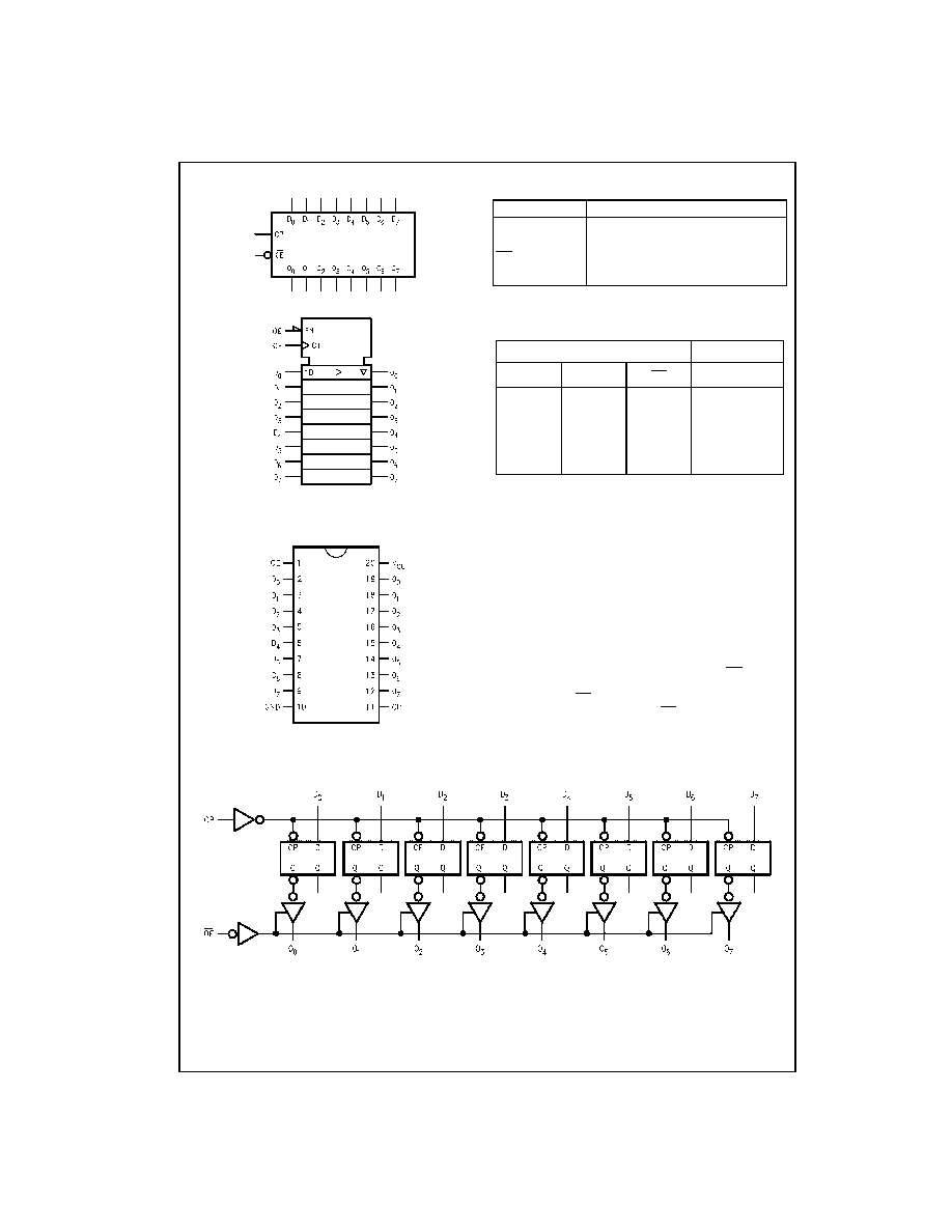
Logic Symbols
IEEE/IEC
Connection Diagram
Pin Descriptions
Truth Table
H
HIGH Voltage Level
L
LOW Voltage Level
X
Immaterial
Z
High Impedance
LOW-to-HIGH Transition
O
o
Previous O
o
before HIGH to LOW of CP
Functional Description
The LVT574 and LVTH574 consist of eight edge-triggered
flip-flops with individual D-type inputs and 3-STATE true
outputs. The buffered clock and buffered Output Enable
are common to all flip-flops. The eight flip-flops will store
the state of their individual D-type inputs that meet the
setup and hold time requirements on the LOW-to-HIGH
Clock (CP) transition. With the Output Enable (OE) LOW,
the contents of the eight flip-flops are available at the out-
puts. When the OE is HIGH, the outputs go to the high
impedance state. Operation of the OE input does not affect
the state of the flip-flops.
Logic Diagram
Please note that this diagram is provided only for the understanding of logic operations and should not be used to estimate propagation delays.
Pin Names
Description
D
0
≠D
7
Data Inputs
CP
Clock Pulse Input
OE
3-STATE Output Enable Input
O
0
≠O
7
3-STATE Outputs
Inputs
Outputs
D
n
CP
OE
O
n
H
L
H
L
L
L
X
L
L
O
o
X
X
H
Z
3
www.fairchildsemi.com
7
4
L
V
T5
74
∑
74L
VTH574
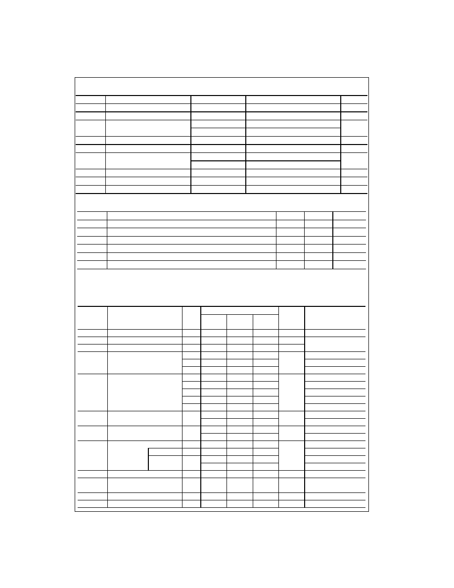
Absolute Maximum Ratings
(Note 2)
Recommended Operating Conditions
Note 2: Absolute Maximum continuous ratings are those values beyond which damage to the device may occur. Exposure to these conditions or conditions
beyond those indicated may adversely affect device reliability. Functional operation under absolute maximum rated conditions is not implied.
Note 3: I
O
Absolute Maximum Rating must be observed.
DC Electrical Characteristics
Symbol
Parameter
Value
Conditions
Units
V
CC
Supply Voltage
0.5 to
4.6
V
V
I
DC Input Voltage
0.5 to
7.0
V
V
O
DC Output Voltage
0.5 to
7.0
Output in 3-STATE
V
0.5 to
7.0
Output in HIGH or LOW State (Note 3)
I
IK
DC Input Diode Current
50
V
I
GND
mA
I
OK
DC Output Diode Current
50
V
O
GND
mA
I
O
DC Output Current
64
V
O
!
V
CC
Output at HIGH State
mA
128
V
O
!
V
CC
Output at LOW State
I
CC
DC Supply Current per Supply Pin
r
64
mA
I
GND
DC Ground Current per Ground Pin
r
128
mA
T
STG
Storage Temperature
65 to
150
q
C
Symbol
Parameter
Min
Max
Units
V
CC
Supply Voltage
2.7
3.6
V
V
I
Input Voltage
0
5.5
V
I
OH
HIGH-Level Output Current
32
mA
I
OL
LOW-Level Output Current
64
mA
T
A
Free-Air Operating Temperature
40
85
q
C
'
t/
'
V
Input Edge Rate, V
IN
0.8V≠2.0V, V
CC
3.0V
0
10
ns/V
Symbol
Parameter
V
CC
(V)
T
A
40
q
C to
85
q
C
Units
Conditions
Min
Typ
Max
(Note 4)
V
IK
Input Clamp Diode Voltage
2.7
1.2
V
I
I
18 mA
V
IH
Input HIGH Voltage
2.7≠3.6
2.0
V
V
O
d
0.1V or
V
IL
Input LOW Voltage
2.7≠3.6
0.8
V
V
O
t
V
CC
0.1V
V
OH
Output HIGH Voltage
2.7≠3.6
V
CC
0.2
V
I
OH
100
P
A
2.7
2.4
I
OH
8 mA
3.0
2.0
I
OH
32 mA
V
OL
Output LOW Voltage
2.7
0.2
V
I
OL
100
P
A
2.7
0.5
I
OL
24 mA
3.0
0.4
I
OL
16 mA
3.0
0.5
I
OL
32 mA
3.0
0.55
I
OL
64 mA
I
I(HOLD)
Bushold Input Minimum Drive
3.0
75
P
A
V
I
0.8V
(Note 5)
75
V
I
2.0V
I
I(OD)
Bushold Input Over-Drive
3.0
500
P
A
(Note 6)
(Note 5)
Current to Change State
500
(Note 7)
I
I
Input Current
3.6
10
P
A
V
I
5.5V
Control Pins
3.6
r
1
V
I
0V or V
CC
Data Pins
3.6
5
V
I
0V
1
V
I
V
CC
I
OFF
Power Off Leakage Current
0
r
100
P
A
0V
d
V
I
or V
O
d
5.5V
I
PU/PD
Power Up/Down 3-STATE
0≠1.5V
r
100
P
A
V
O
0.5V to 3.0V
Output Current
V
I
GND or V
CC
I
OZL
3-STATE Output Leakage Current
3.6
5
P
A
V
O
0.5V
I
OZH
3-STATE Output Leakage Current
3.6
5
P
A
V
O
3.0V
www.fairchildsemi.com
4
74L
VT574
∑
74
L
V
TH574
DC Electrical Characteristics
(Continued)
Note 4: All typical values are at V
CC
3.3V, T
A
25
q
C.
Note 5: Applies to bushold versions only (74LVTH574).
Note 6: An external driver must source at least the specified current to switch from LOW-to-HIGH.
Note 7: An external driver must sink at least the specified current to switch from HIGH-to-LOW.
Note 8: This is the increase in supply current for each input that is at the specified voltage level rather than V
CC
or GND.
Dynamic Switching Characteristics
(Note 9)
Note 9: Characterized in SOIC package. Guaranteed parameter, but not tested.
Note 10: Max number of outputs defined as (n). n
1 data inputs are driven 0V to 3V. Output under test held LOW.
AC Electrical Characteristics
Note 11: All typical values are at V
CC
3.3V, T
A
25
q
C.
Note 12: Skew is defined as the absolute value of the difference between the actual propagation delay for any two separate outputs of the same device. The
specification applies to any outputs switching in the same direction, either HIGH to LOW (t
OSHL
) or LOW to HIGH (t
OSLH
).
Capacitance
(Note 13)
Note 13: Capacitance is measured at frequency f
1 MHz, per MIL-STD-883, Method 3012.
Symbol
Parameter
V
CC
(V)
T
A
40
q
C to
85
q
C
Units
Conditions
Min
Typ
Max
(Note 4)
I
OZH
3-STATE Output Leakage Current
3.6
10
P
A
V
CC
V
O
d
5.5V
I
CCH
Power Supply Current
3.6
0.19
mA
Outputs High
I
CCL
Power Supply Current
3.6
5
mA
Outputs Low
I
CCZ
Power Supply Current
3.6
0.19
mA
Outputs Disabled
I
CCZ
Power Supply Current
3.6
0.19
mA
V
CC
d
V
O
d
5.5V,
Outputs Disabled
'
I
CC
Increase in Power Supply Current
3.6
0.2
mA
One Input at V
CC
0.6V
(Note 8)
Other Inputs at V
CC
or GND
Symbol
Parameter
V
CC
T
A
25
q
C
Units
Conditions
(V)
Min
Typ
Max
C
L
50 pF, R
L
500
:
V
OLP
Quiet Output Maximum Dynamic V
OL
3.3
0.8
V
(Note 10)
V
OLV
Quiet Output Minimum Dynamic V
OL
3.3
0.8
V
(Note 10)
Symbol
Parameter
T
A
40
q
C to
85
q
C
C
L
50 pF, R
L
500
:
Units
V
CC
3.3V
r
0.3V
V
CC
2.7V
Min
Typ
(Note 11)
Max
Min
Max
f
MAX
Maximum Clock Frequency
150
150
MHz
t
PHL
Propagation Delay
1.8
4.6
1.8
5.3
ns
t
PLH
CP to O
n
1.8
4.5
1.8
5.3
t
PZL
Output Enable Time
1.5
5.2
1.5
6.1
ns
t
PZH
1.5
4.8
1.5
5.9
t
PLZ
Output Disable Time
2.0
4.4
2.0
4.4
ns
t
PHZ
2.0
4.8
2.0
5.1
t
S
Setup Time
2.0
2.4
ns
t
H
Hold Time
0.3
0.0
ns
t
W
Pulse Width
3.3
3.3
ns
t
OSHL
Output to Output Skew (Note 12)
1.0
1.0
ns
t
OSLH
1.0
1.0
Symbol
Parameter
Conditions
Typical
Units
C
IN
Input Capacitance
V
CC
Open, V
I
0V or V
CC
4
pF
C
OUT
Output Capacitance
V
CC
3.0V, V
O
0V or V
CC
6
pF
5
www.fairchildsemi.com
7
4
L
V
T5
74
∑
74L
VTH574
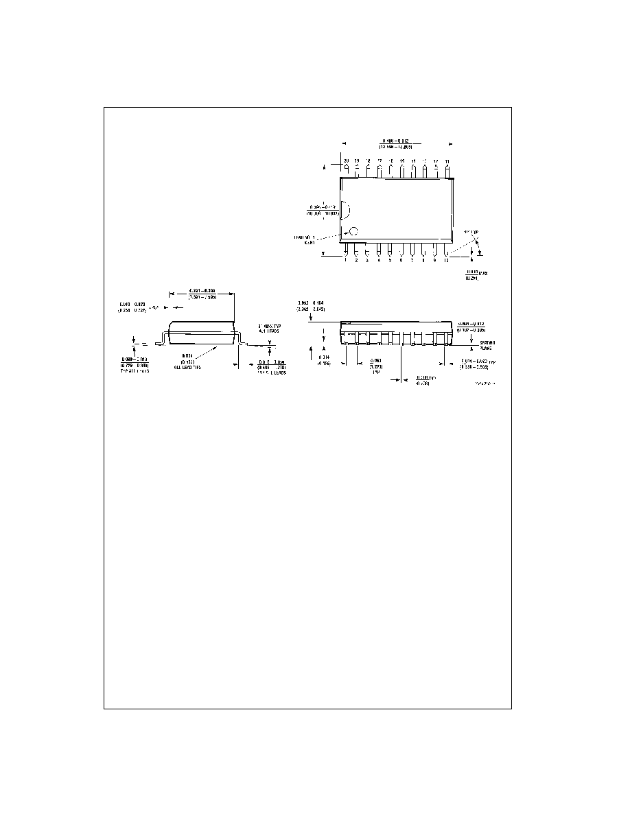
Physical Dimensions
inches (millimeters) unless otherwise noted
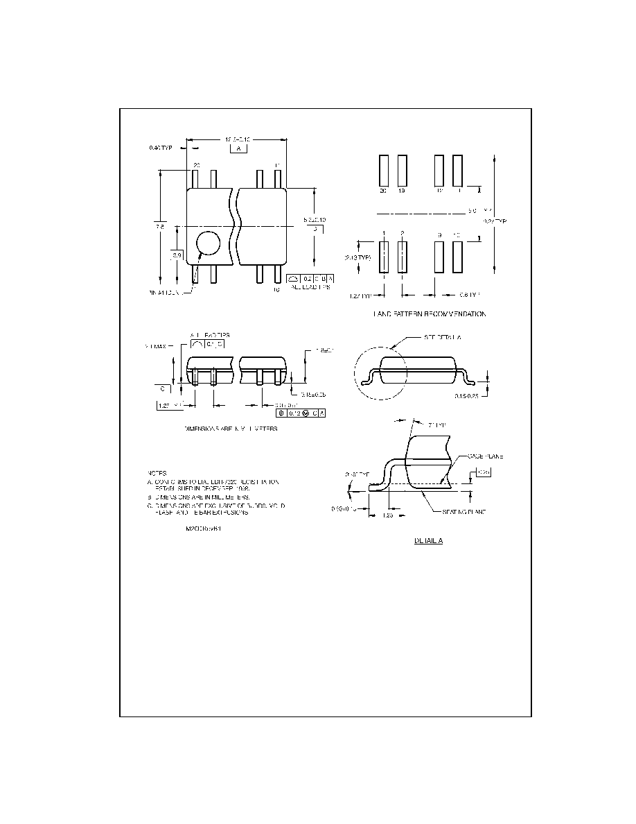
20-Lead Small Outline Integrated Circuit (SOIC), JEDEC MS-013, 0.300" Wide
Package Number M20B
www.fairchildsemi.com
6
74L
VT574
∑
74
L
V
TH574
Physical Dimensions
inches (millimeters) unless otherwise noted (Continued)
Pb-Free 20-Lead Small Outline Package (SOP), EIAJ TYPE II, 5.3mm Wide
Package Number M20D
7
www.fairchildsemi.com
7
4
L
V
T5
74
∑
74L
VTH574
Physical Dimensions
inches (millimeters) unless otherwise noted (Continued)
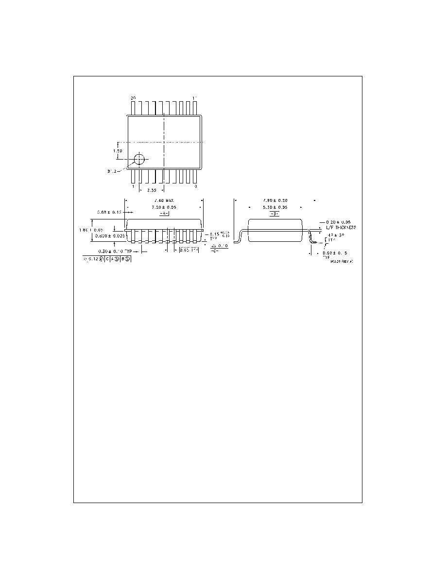
20-Lead Shrink Small Outline Package (SSOP), JEDEC MO-150, 5.3mm Wide
Package Number MSA20
www.fairchildsemi.com
8
74L
VT574
∑
74
L
V
TH574
Low V
o
l
t
age Oct
a
l D-T
ype Fl
ip-
F
lop wit
h
3-
ST
A
T
E Output
s
Physical Dimensions
inches (millimeters) unless otherwise noted (Continued)
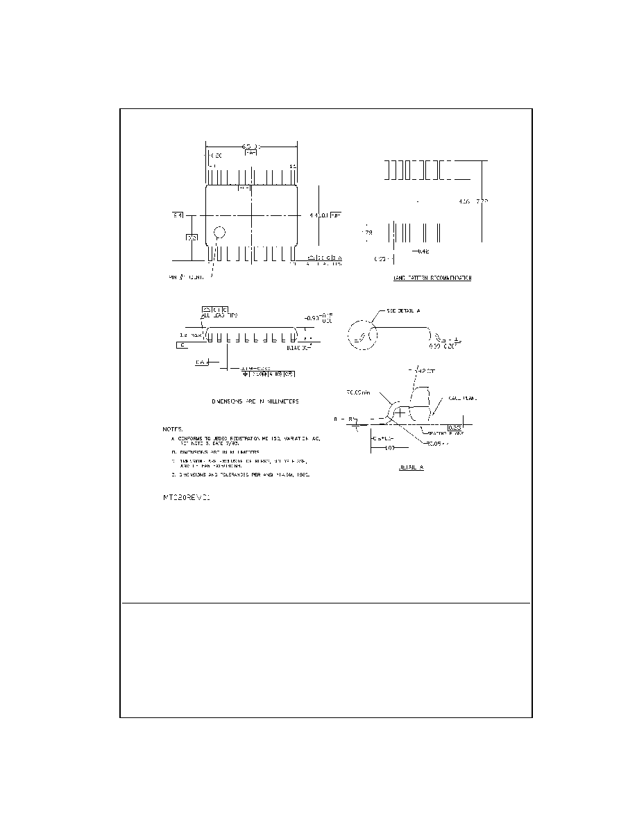
20-Lead Thin Shrink Small Outline Package (TSSOP), JEDEC MO-153, 4.4mm Wide
Package Number MTC20
Fairchild does not assume any responsibility for use of any circuitry described, no circuit patent licenses are implied and
Fairchild reserves the right at any time without notice to change said circuitry and specifications.
LIFE SUPPORT POLICY
FAIRCHILD'S PRODUCTS ARE NOT AUTHORIZED FOR USE AS CRITICAL COMPONENTS IN LIFE SUPPORT
DEVICES OR SYSTEMS WITHOUT THE EXPRESS WRITTEN APPROVAL OF THE PRESIDENT OF FAIRCHILD
SEMICONDUCTOR CORPORATION. As used herein:
1. Life support devices or systems are devices or systems
which, (a) are intended for surgical implant into the
body, or (b) support or sustain life, and (c) whose failure
to perform when properly used in accordance with
instructions for use provided in the labeling, can be rea-
sonably expected to result in a significant injury to the
user.
2. A critical component in any component of a life support
device or system whose failure to perform can be rea-
sonably expected to cause the failure of the life support
device or system, or to affect its safety or effectiveness.
www.fairchildsemi.com