© 2005 Fairchild Semiconductor Corporation
DS011551
www.fairchildsemi.com
February 1993
Revised February 2005
7
4
L
VX00
Low V
o
l
t
age
Q
u
ad 2-
Inpu
t
N
AND
G
a
te
74LVX00
Low Voltage Quad 2-Input NAND Gate
General Description
The LVX00 contains four 2-input NAND gates. The inputs
tolerate voltages up to 7V allowing the interface of 5V sys-
tems to 3V systems.
Features
s
Input voltage level translation from 5V to 3V
s
Ideal for low power/low noise 3.3V applications
s
Guaranteed simultaneous switching noise level and
dynamic threshold performance
Ordering Code:
Devices also available in Tape and Reel. Specify by appending suffix letter "X" to the ordering code.
Pb-Free package per JEDEC J-STD-020B.
Note 1: "_NL" indicates Pb-Free package (per JEDEC J-STD-020B). Device available in Tape and Reel only.
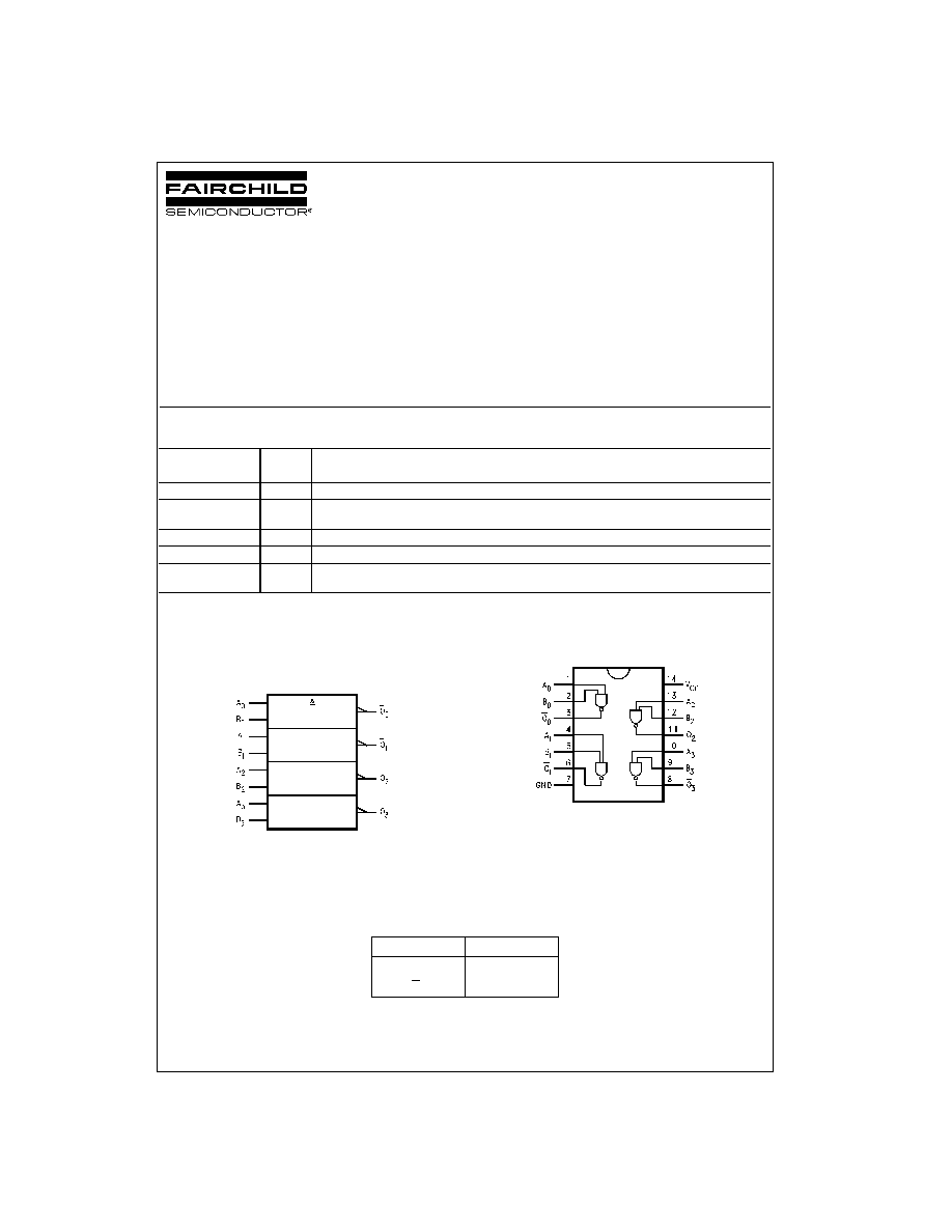
Logic Symbol
IEEE/IEC
Connection Diagram
Pin Descriptions
Order Number
Package
Package Description
Number
74LVX00M
M14A
14-Lead Small Outline Integrated Circuit (SOIC), JEDEC MS-012, 0.150" Narrow
74LVX00MX_NL
(Note 1)
M14A
Pb-Free 14-Lead Small Outline Integrated Circuit (SOIC), JEDEC MS-012, 0.150" Narrow
74LVX00SJ
M14D
Pb-Free 14-Lead Small Outline Package (SOP), EIAJ TYPE II, 5.3mm Wide
74LVX00MTC
MTC14
14-Lead Thin Shrink Small Outline Package (TSSOP), JEDEC MO-153, 4.4mm Wide
74LVX00MTCX_NL
(Note 1)
MTC14
Pb-Free 14-Lead Thin Shrink Small Outline Package (TSSOP), JEDEC MO-153, 4.4mm Wide
Pin Names
Description
A
n
, B
n
Inputs
O
n
Outputs
www.fairchildsemi.com
2
74
L
V
X
0
0
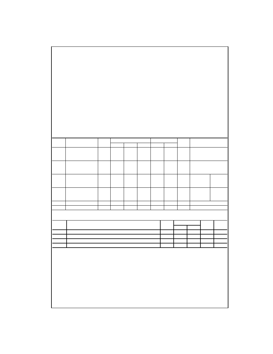
Absolute Maximum Ratings
(Note 2)
Recommended Operating
Conditions
(Note 3)
Note 2: The "Absolute Maximum Ratings" are those values beyond which
the safety of the device cannot be guaranteed. The device should not be
operated at these limits. The parametric values defined in the Electrical
Characteristics tables are not guaranteed at the absolute maximum ratings.
The "Recommended Operating Conditions" table will define the conditions
for actual device operation.
Note 3: Unused inputs must be held HIGH or LOW They may not float.
DC Electrical Characteristics
Noise Characteristics
(Note 4)
Note 4: Input t
r
t
f
3ns
Supply Voltage (V
CC
)
0.5V to
7.0V
DC Input Diode Current (I
IK
)
V
I
0.5V
20 mA
DC Input Voltage (V
I
)
0.5V to 7V
DC Output Diode Current (I
OK
)
V
O
0.5V
20 mA
V
O
V
CC
0.5V
20 mA
DC Output Voltage (V
O
)
0.5V to V
CC
0.5V
DC Output Source
or Sink Current (I
O
)
r
25 mA
DC V
CC
or Ground Current
(I
CC
or I
GND
)
r
50 mA
Storage Temperature (T
STG
)
65
q
C to
150
q
C
Power Dissipation
180 mW
Supply Voltage (V
CC
)
2.0V to 3.6V
Input Voltage (V
I
)
0V to 5.5V
Output Voltage (V
O
)
0V to V
CC
Operating Temperature (T
A
)
40
q
C to
85
q
C
Input Rise and Fall Time (
'
t/
'
V)
0 ns/V to 100 ns/V
Symbol
Parameter
V
CC
T
A
25
q
C
T
A
40
q
C to
85
q
C
Units
Conditions
Min
Typ
Max
Min
Max
V
IH
HIGH Level Input
2.0
1.5
1.5
Voltage
3.0
2.0
2.0
V
3.6
2.4
2.4
V
IL
LOW Level Input
2.0
0.5
0.5
Voltage
3.0
0.8
0.8
V
3.6
0.8
0.8
V
OH
HIGH Level Output
2.0
1.9
2.0
1.9
V
IN
V
IL
or V
IH
I
OH
50
P
A
Voltage
3.0
2.9
3.0
2.9
V
I
OH
50
P
A
3.0
2.58
2.48
I
OH
4 mA
V
OL
LOW Level Output
2.0
0.0
0.1
0.1
V
IN
V
IL
or V
IH
I
OL
50
P
A
Voltage
3.0
0.0
0.1
0.1
V
I
OL
50
P
A
3.0
0.36
0.44
I
OL
4 mA
I
IN
Input Leakage Current
3.6
r
0.1
r
1.0
P
A
V
IN
5.5V or GND
I
CC
Quiescent Supply Current
3.6
2.0
20.0
P
A
V
IN
V
CC
or GND
Symbol
Parameter
V
CC
T
A
25
q
C
Units
C
L
(pF)
(V)
Typ
Limit
V
OLP
Quiet Output Maximum Dynamic V
OL
3.3
0.3
0.5
V
50
V
OLV
Quiet Output Minimum Dynamic V
OL
3.3
0.3
0.5
V
50
V
IHD
Minimum HIGH Level Dynamic Input Voltage
3.3
2.0
V
50
V
ILD
Maximum LOW Level Dynamic Input Voltage
3.3
0.8
V
50
3
www.fairchildsemi.com
7
4
L
VX00
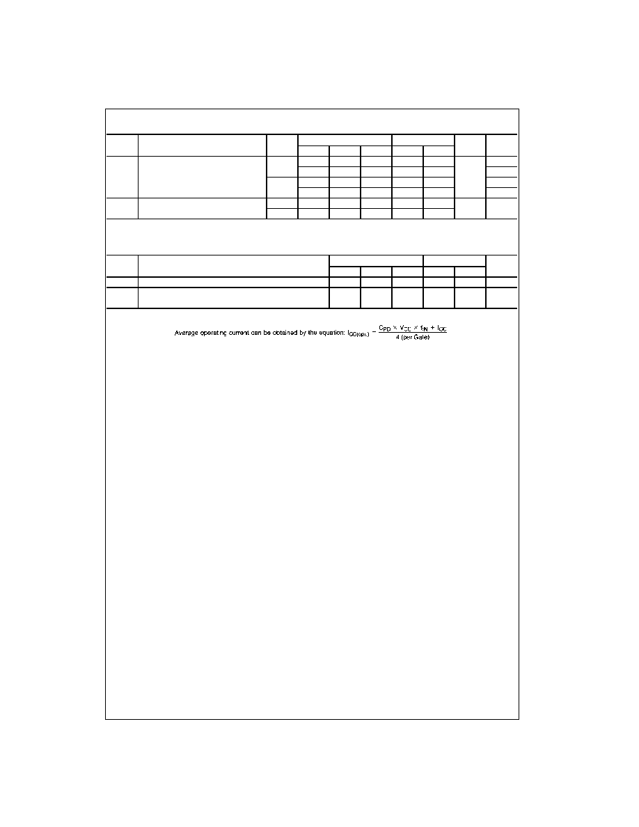
AC Electrical Characteristics
Note 5: Parameter guaranteed by design t
OSLH
|t
PLHm
≠t
PLHn
|, t
OSHL
|t
PHLm
≠t
PHLn
|
Capacitance
Note 6: C
PD
is defined as the value of the internal equivalent capacitance which is calculated from the operating current consumption without load.
Symbol
Parameter
V
CC
T
A
25
q
C
T
A
40
q
C to
85
q
C
Units
C
L
(pF)
(V)
Min
Typ
Max
Min
Max
t
PLH
Propagation Delay Time
2.7
5.4
10.1
1.0
12.5
ns
15
t
PHL
7.9
13.6
1.0
16.0
50
3.3
r
0.3
4.1
6.2
1.0
7.5
15
6.6
9.7
1.0
11.0
50
t
OSLH
Output to Output Skew
2.7
1.5
1.5
ns
50
t
OSHL
(Note 5)
3.3
1.5
1.5
Symbol
Parameter
T
A
25
q
C
T
A
40
q
C to
85
q
C
Units
Min
Typ
Max
Min
Max
C
IN
Input Capacitance
4
10
10
pF
C
PD
Power Dissipation
19
pF
Capacitance (Note 6)
www.fairchildsemi.com
4
74
L
V
X
0
0
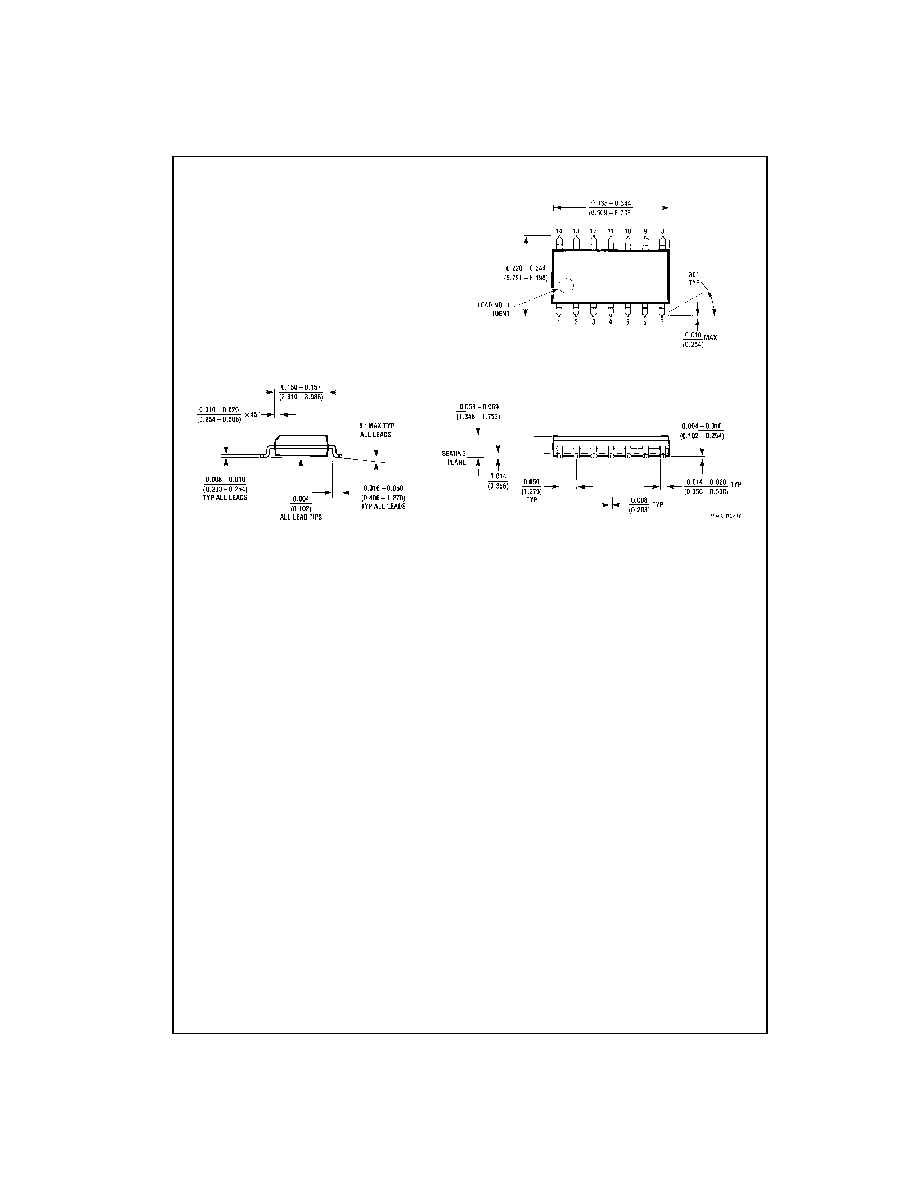
Physical Dimensions
inches (millimeters) unless otherwise noted
14-Lead Small Outline Integrated Circuit (SOIC), JEDEC MS-012, 0.150" Narrow
Package Number M14A
5
www.fairchildsemi.com
7
4
L
VX00
Physical Dimensions
inches (millimeters) unless otherwise noted (Continued)
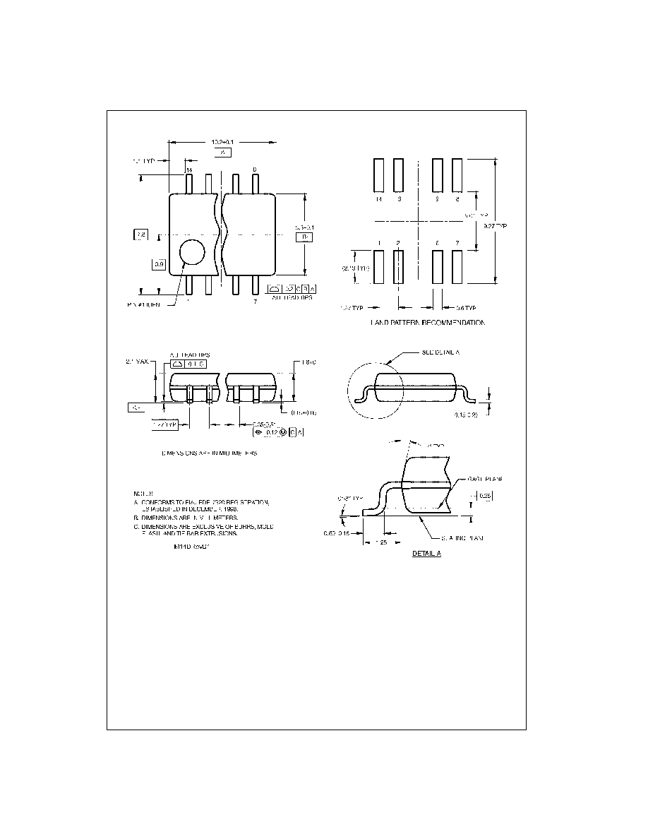
Pb-Free 14-Lead Small Outline Package (SOP), EIAJ TYPE II, 5.3mm Wide
Package Number M14D