© 2003 Fairchild Semiconductor Corporation
DS012158
www.fairchildsemi.com
October 1996
Revised December 2003
7
4
L
VX1
1
2
Low
V
o
l
t
a
g
e Dual
J-
K Fl
i
p
-Fl
ops
w
i
th
Prese
t
and Cl
ear
74LVX112
Low Voltage Dual J-K Flip-Flops with Preset and Clear
General Description
The LVX112 is a dual J-K Flip-Flop where each flip-flop has
independent inputs (J, K, PRESET, CLEAR, and CLOCK)
and outputs (Q, Q). These devices are edge sensitive and
change states synchronously on the negative going transi-
tion of the clock pulse. Triggering occurs at a voltage level
of the clock and is not directly related to the transition time.
Clear and Preset are independent of the clock and are
accomplished by a low logic level on the corresponding
input. The J and K inputs can change when the clock is in
either state without affecting the flip-flop, provided that they
are in the desired state during the recommended setup and
hold times relative to the falling edge of the clock.
The inputs tolerate voltages up to 7V allowing the interface
of 5V systems to 3V systems.
Features
s
Input voltage level translation from 5V≠3V
s
Ideal for low power/low noise 3.3V applications
Ordering Code:
Devices also available in Tape and Reel. Specify by appending suffix letter "X" to the ordering code.
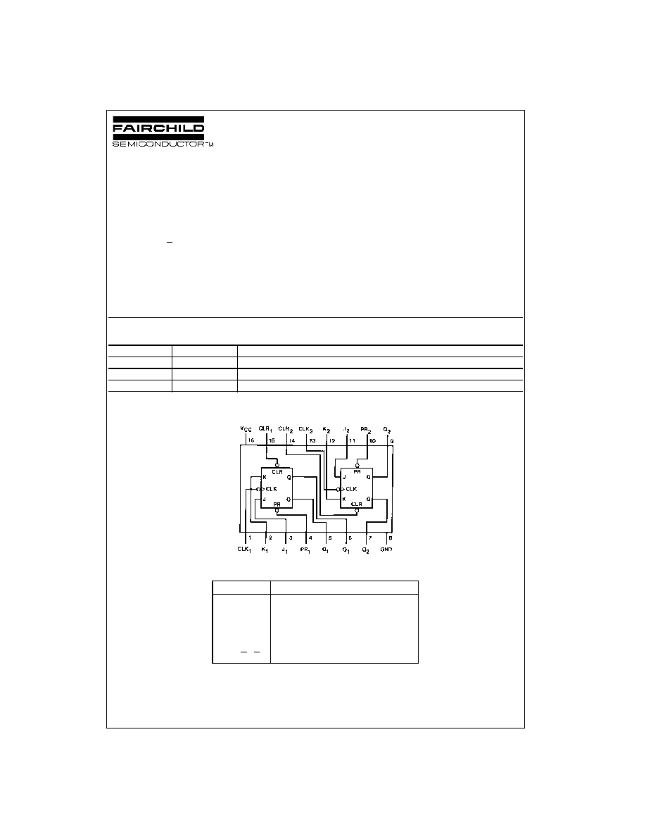
Connection Diagram
Pin Descriptions
Order Number
Package Number
Package Description
74LVX112M
M16A
16-Lead Small Outline Integrated Circuit (SOIC), JEDEC MS-012, 0.150" Narrow
74LVX112SJ
M16D
16-Lead Small Outline Package (SOP), EIAJ TYPE II, 5.3mm Wide
74LVX112MTC
MTC16
16-Lead Thin Shrink Small Outline Package (TSSOP), JEDEC MO-153, 4.4mm Wide
Pin Names
Description
J
1
, J
2
, K
1
, K
2
Data Inputs
CLK
1
, CLK
2
Clock Pulse Inputs (Active Falling edge)
CLR
1
, CLR
2
Direct Clear Inputs (Active LOW)
PR
1
, PR
2
Direct Preset Inputs (Active LOW)
Q
1
, Q
2
, Q
1
, Q
2

www.fairchildsemi.com
2
74
L
VX1
12
Truth Table
H (h)
=
HIGH Voltage Level
L (l)
=
LOW Voltage Level
X
=
Immaterial
=
HIGH-to-LOW Clock Transition
Q
0
(Q
0
)
=
Before HIGH-to-LOW Transition of Clock
Lower case letters indicate the state of the referenced input or output one setup time prior to the HIGH-to-LOW clock transition.
Logic Diagram
(One Half Shown)
Inputs
Outputs
PR
CLR
CP
J
K
Q
Q
L
H
X
X
X
H
L
H
L
X
X
X
L
H
L
L
X
X
X
H
H
H
H
h
h
Q
0
Q
0
H
H
l
h
L
H
H
H
h
l
H
L
H
H
l
l
Q
0
Q
0

3
www.fairchildsemi.com
74
L
V
X
1
12
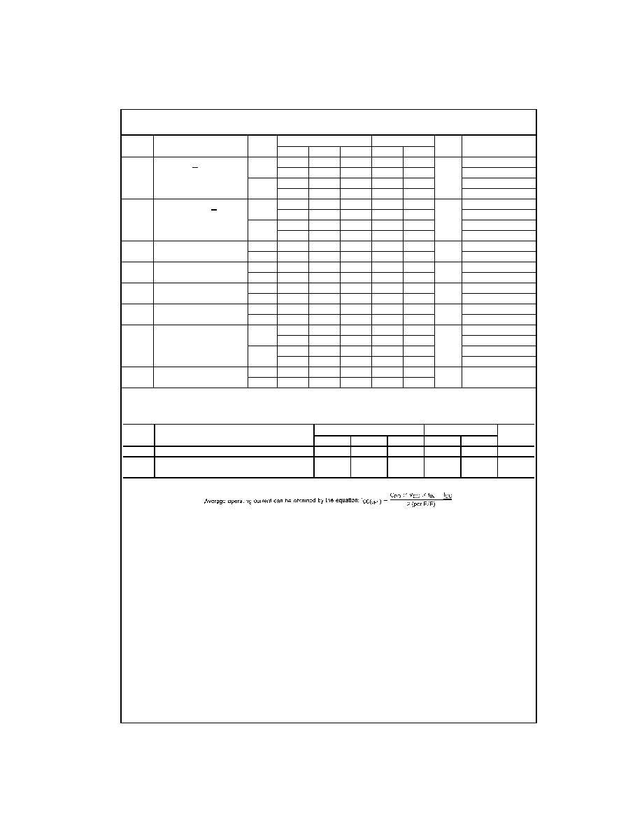
Absolute Maximum Ratings
(Note 1)
Recommended Operating
Conditions
(Note 2)
Note 1: The "Absolute Maximum Ratings" are those values beyond which
the safety of the device cannot be guaranteed. The device should not be
operated at these limits. The parametric values defined in the Electrical
Characteristics tables are not guaranteed at the absolute maximum ratings.
The "Recommended Operating Conditions" table will define the conditions
for actual device operation.
Note 2: Unused inputs must be held HIGH or LOW. They may not float.
DC Electrical Characteristics
Supply Voltage (V
CC
)
-
0.5V to
+
7.0V
DC Input Diode Current (I
IK
)
V
I
=
-
0.5V
-
20 mA
DC Input Voltage (V
I
)
-
0.5V to 7V
DC Output Diode Current (I
OK
)
V
O
=
-
0.5V
-
20 mA
V
O
=
V
CC
+
0.5V
+
20 mA
DC Output Voltage (V
O
)
-
0.5V to V
CC
+
0.5V
DC Output Source
or Sink Current (I
O
)
±
25 mA
DC V
CC
or Ground Current
(I
CC
or I
GND
)
±
50 mA
Storage Temperature (T
STG
)
-
65
∞
C to
+
150
∞
C
Power Dissipation
180 mW
Supply Voltage (V
CC
)
2.0V to 3.6V
Input Voltage (V
I
)
0V to 5.5V
Output Voltage (V
O
)
0V to V
CC
Operating Temperature (T
A
)
-
40
∞
C to
+
85
∞
C
Input Rise and Fall Time (
t/
V)
0 ns/V to 100 ns/V
Symbol
Parameter
V
CC
T
A
=
+
25
∞
C
T
A
=
-
40
∞
C to
+
85
∞
C
Units
Conditions
Min
Typ
Max
Min
Max
V
IH
HIGH Level
2.0
1.5
1.5
Input Voltage
3.0
2.0
2.0
V
3.6
2.4
2.4
V
IL
LOW Level
2.0
0.5
0.5
Input Voltage
3.0
0.8
0.8
V
3.6
0.8
0.8
V
OH
HIGH Level
2.0
1.9
2.0
1.9
V
IN
=
V
IL
or V
IH
I
OH
=
-
50
µ
A
Output Voltage
3.0
2.9
3.0
2.9
V
I
OH
=
-
50
µ
A
3.0
2.58
2.48
I
OH
=
-
4 mA
V
OL
Low Level
2.0
0.0
0.1
0.1
V
IN
=
V
IL
or V
IH
I
OL
=
50
µ
A
Output Voltage
3.0
0.0
0.1
0.1
V
I
OL
=
50
µ
A
3.0
0.36
0.44
I
OL
=
4 mA
I
IN
Input Leakage Current
3.6
±
0.1
±
1.0
µ
A
V
IN
=
5.5V or GND
I
CC
Quiescent Supply Current
3.6
2.0
20.0
µ
A
V
IN
=
V
CC
or GND
www.fairchildsemi.com
4
74
L
VX1
12
AC Electrical Characteristics
Note 3: Parameter guaranteed by design. t
OSLH
=
|t
PLHm
≠t
PLHn
|, t
OSLH
=
|t
PHLm
≠t
PHLn
|
Capacitance
Note 4: C
PD
is defined as the value of the internal equivalent capacitance which is calculated from the operating current consumption without load.
Symbol
Parameter
V
CC
T
A
=
+
25
∞
C
T
A
=
-
40
∞
C to
+
85
∞
C
Units
C
L
(pF)
(V)
Min
Typ
Max
Min
Max
t
PLH
Propagation Delay
2.7
7.5
12.0
1.0
14.2
ns
15
t
PHL
CP
n
to Q
n
or Q
n
11.0
16.7
1.0
19.0
50
3.3
±
0.3
8.5
11.0
1.0
13.4
15
10.0
15.0
1.0
16.5
50
t
PLH
Propagation Delay
2.7
7.0
11.5
1.0
12.3
ns
15
t
PHL
PR or CLR to Q
n
or Q
n
10.1
14.3
1.0
16.5
50
3.3
±
0.3
6.7
10.2
1.0
11.7
15
9.7
13.5
1.0
15.0
50
t
W
Pulse Width
2.7
5.0
5.0
ns
(CP or CLR or PR)
3.3
±
0.3
5.0
5.0
t
S
Setup Time
2.7
5.5
5.5
ns
(J
n
or K
n
to CP
n
)
3.3
±
0.3
5.0
5.0
t
H
Hold Time
2.7
1.0
1.0
ns
(J
n
or K
n
to CP
n
)
3.3
±
0.3
1.0
1.0
t
REC
Recovery Time
2.7
6.5
6.5
ns
(CLR or PR to CP)
3.3
±
0.3
6.0
6.0
f
MAX
Maximum Clock
2.7
90
140
85
MHz
15
Frequency
85
115
70
50
3.3
±
0.3
110
150
100
15
90
120
80
50
t
OSLH
,
Output to Output Skew
2.7
1.5
1.5
ns
50
t
OSHL
(Note 3)
3.3
1.5
1.5
Symbol
Parameter
T
A
=
+
25
∞
C
T
A
=
-
40
∞
C to
+
85
∞
C
Units
Min
Typ
Max
Min
Max
C
IN
Input Capacitance
4
10
10
pF
C
PD
Power Dissipation
18
pF
Capacitance (Note 4)

5
www.fairchildsemi.com
74
L
V
X
1
12
Physical Dimensions
inches (millimeters) unless otherwise noted
16-Lead Small Outline Integrated Circuit (SOIC), JEDEC MS-012, 0.150" Narrow
Package Number M16A