© 2003 Fairchild Semiconductor Corporation
DS011615
www.fairchildsemi.com
June 1993
Revised October 2003
7
4
L
VX13
8
Low
V
o
l
t
a
g
e 1-
of-
8
D
e
coder/
Dem
u
l
t
i
p
l
exer
74LVX138
Low Voltage 1-of-8 Decoder/Demultiplexer
General Description
The LVX138 is a high-speed 1-of-8 decoder/demultiplexer.
This device is ideally suited for high-speed bipolar memory
chip select address decoding. The multiple input enables
allow parallel expansion to a 1-of-24 decoder using just
three LVX138 devices or a 1-of-32 decoder using four
LVX138 devices and one inverter.
Features
s
Input voltage level translation from 5V to 3V
s
Ideal for low power/low noise 3.3V applications
s
Guaranteed simultaneous switching noise level and
dynamic threshold performance
Ordering Code:
Devices also available in Tape and Reel. Specify by appending suffix letter "X" to the ordering code.
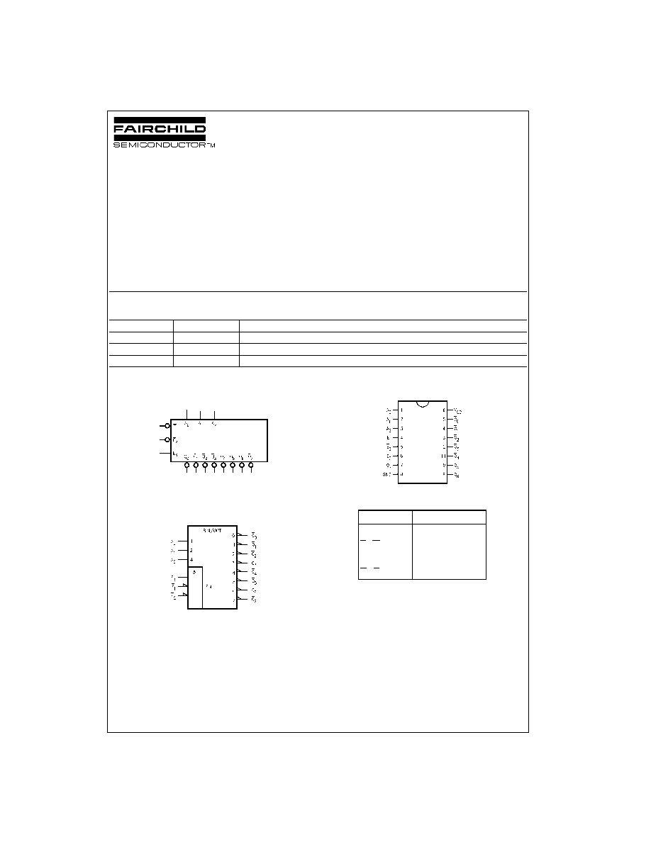
Logic Symbols
IEEE/IEC
Connection Diagram
Pin Descriptions
Order Number
Package Number
Package Description
74LVX138M
M16A
16-Lead Small Outline Integrated Circuit (SOIC), JEDEC MS-012, 0.150" Narrow
74LVX138SJ
M16D
16-Lead Small Outline Package (SOP), EIAJ TYPE II, 5.3mm Wide
74LVX138MTC
MTC16
16-Lead Thin Shrink Small Outline Package (TSSOP), JEDEC MO-153, 4.4mm Wide
Pin Names
Description
A
0
≠A
2
Address Inputs
E
1
≠ E
2
Enable Inputs
E
3
Enable Input
O
0
≠O
7
Outputs
www.fairchildsemi.com
2
74
L
VX138
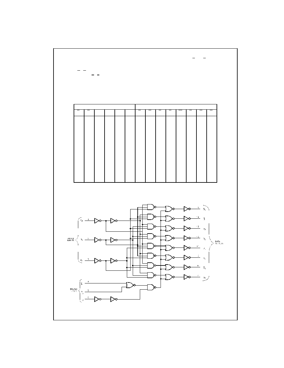
Functional Description
The LVX138 high-speed 1-of-8 decoder/demultiplexer
accepts three binary weighted inputs (A
0
, A
1
, A
2
) and,
when enabled, provides eight mutually exclusive active-
LOW outputs (O
0
≠O
7
). The LVX138 features three Enable
inputs, two active-LOW (E
1
, E
2
) and one active-HIGH (E
3
).
All outputs will be HIGH unless E
1
and E
2
are LOW and E
3
is HIGH.
The LVX138 can be used as an 8-output demultiplexer by
using one of the active LOW Enable inputs as the data
input and the other Enable inputs as strobes. The Enable
inputs which are not used must be permanently tied to their
appropriate active-HIGH or active-LOW state.
Truth Table
H
=
HIGH Voltage Level
L
=
LOW Voltage Level
X
=
Immaterial
Logic Diagram
Please note that this diagram is provided only for the understanding of logic operations and should not be used to estimate propagation delays.
Inputs
Outputs
E
1
E
2
E
3
A
0
A
1
A
2
O
0
O
1
O
2
O
3
O
4
O
5
O
6
O
7
H
X
X
X
X
X
H
H
H
H
H
H
H
H
X
H
X
X
X
X
H
H
H
H
H
H
H
H
X
X
L
X
X
X
H
H
H
H
H
H
H
H
L
L
H
L
L
L
L
H
H
H
H
H
H
H
L
L
H
H
L
L
H
L
H
H
H
H
H
H
L
L
H
L
H
L
H
H
L
H
H
H
H
H
L
L
H
H
H
L
H
H
H
L
H
H
H
H
L
L
H
L
L
H
H
H
H
H
L
H
H
H
L
L
H
H
L
H
H
H
H
H
H
L
H
H
L
L
H
L
H
H
H
H
H
H
H
H
L
H
L
L
H
H
H
H
H
H
H
H
H
H
H
L
3
www.fairchildsemi.com
74
L
V
X
1
38
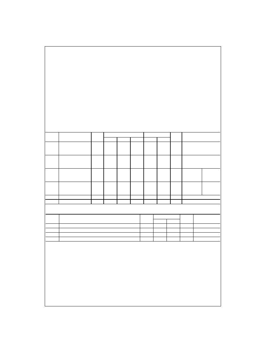
Absolute Maximum Ratings
(Note 1)
Recommended Operating
Conditions
(Note 2)
Note 1: The "Absolute Maximum Ratings" are those values beyond which
the safety of the device cannot be guaranteed. The device should not be
operated at these limits. The parametric values defined in the Electrical
Characteristics tables are not guaranteed at the absolute maximum ratings.
The "Recommended Operating Conditions" table will define the conditions
for actual device operation.
Note 2: Unused inputs must be held HIGH or LOW. They may not float.
DC Electrical Characteristics
Noise Characteristics
(Note 3)
Note 3: Input t
r
=
t
f
=
3 ns
Supply Voltage (V
CC
)
-
0.5V to
+
7.0V
DC Input Diode Current (I
IK
)
V
I
=
-
0.5V
-
20 mA
DC Input Voltage (V
I
)
-
0.5V to 7V
DC Output Diode Current (I
OK
)
V
O
=
-
0.5V
-
20 mA
V
O
=
V
CC
+
0.5V
+
20 mA
DC Output Voltage (V
O
)
-
0.5V to V
CC
+
0.5V
DC Output Source
or Sink Current (I
O
)
±
25 mA
DC V
CC
or Ground Current (I
CC
or I
GND
)
±
75 mA
Storage Temperature (T
STG
)
-
65
∞
C to
+
150
∞
C
Power Dissipation
180 mW
Supply Voltage (V
CC
)
2.0V to 3.6V
Input Voltage (V
I
)
0V to 5.5V
Output Voltage (V
O
)
0V to V
CC
Operating Temperature (T
A
)
-
40
∞
C to
+
85
∞
C
Input Rise and Fall Time (
t/
V)
0 ns/V to 100 ns/V
Symbol
Parameter
V
CC
T
A
=
+
25
∞
C
T
A
=
-
40
∞
C to
+
85
∞
C
Units
Conditions
Min
Typ
Max
Min
Max
V
IH
HIGH Level
2.0
1.5
1.5
Input Voltage
3.0
2.0
2.0
V
3.6
2.4
2.4
V
IL
LOW Level
2.0
0.5
0.5
Input Voltage
3.0
0.8
0.8
V
3.6
0.8
0.8
V
OH
HIGH Level
2.0
1.9
2.0
1.9
V
IN
=
V
IL
or V
IH
I
OH
=
-
50
µ
A
Output Voltage
3.0
2.9
3.0
2.9
V
I
OH
=
-
50
µ
A
3.0
2.58
2.48
I
OH
=
-
4 mA
V
OL
LOW Level
2.0
0.0
0.1
0.1
V
IN
=
V
IL
or V
IH
I
OL
=
50
µ
A
Output Voltage
3.0
0.0
0.1
0.1
V
I
OL
=
50
µ
A
3.0
0.36
0.44
I
OL
=
4 mA
I
IN
Input Leakage Current
3.6
±
0.1
±
1.0
µ
A
V
IN
=
5.5V or GND
I
CC
Quiescent Supply Current
3.6
4.0
40.0
µ
A
V
IN
=
V
CC
or GND
Symbol
Parameter
V
CC
T
A
=
25
∞
C
Units
C
L
(pF)
(V)
Typ
Limit
V
OLP
Quiet Output Maximum Dynamic V
OL
3.3
0.3
0.5
V
50
V
OLV
Quiet Output Minimum Dynamic V
OL
3.3
-
0.3
-
0.5
V
50
V
IHD
Minimum HIGH Level Dynamic Input Voltage
3.3
2.0
V
50
V
ILD
Maximum LOW Level Dynamic Input Voltage
3.3
0.8
V
50
www.fairchildsemi.com
4
74
L
VX138
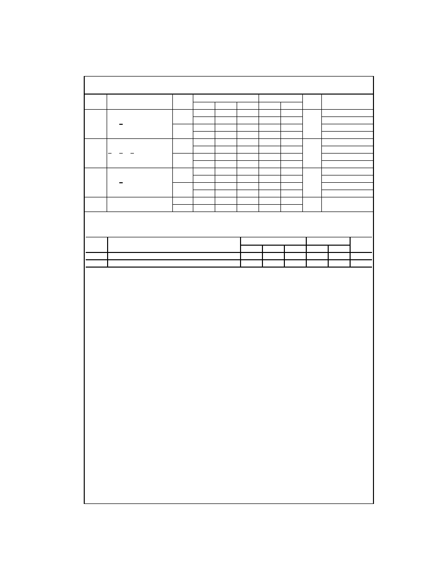
AC Electrical Characteristics
Note 4: Parameter guaranteed by design. t
OSLH
=
|t
PLHm
≠t
PLHn
|, t
OSHL
=
|t
PHLm
≠t
PHLn
|
Capacitance
Note 5: C
PD
is defined as the value of the internal equivalent capacitance which is calculated from the operating current consumption without load.
Average operating current can be obtained by the equation: C
PD
◊
V
CC
◊
I
IN
+
I
CC
Symbol
Parameter
V
CC
T
A
=
+
25
∞
C
T
A
=
-
40
∞
C to
+
85
∞
C
Units
CL (pF)
(V)
Min
Typ
Max
Min
Max
t
PLH
Propagation
2.7
7.1
13.8
1.0
16.5
ns
15
t
PHL
Delay Time
9.6
17.3
1.0
20.0
50
A
n
to O
n
3.3
±
0.3
5.5
8.8
1.0
10.5
15
8.0
12.3
1.0
14.0
50
t
PLH
Propagation
2.7
8.8
16.0
1.0
18.5
ns
15
t
PHL
Delay Time
11.3
19.5
1.0
22.0
50
E
1
or E
2
to O
n
3.3
±
0.3
6.9
10.4
1.0
11.5
15
9.4
13.9
1.0
15.0
50
t
PLH
Propagation
2.7
8.7
16.3
1.0
19.5
ns
15
t
PHL
Delay Time
11.2
19.8
1.0
23.0
50
E
3
to O
n
3.3
±
0.3
6.8
10.6
1.0
12.5
15
9.3
14.1
1.0
16.0
50
t
OSHL
Output to Output
2.7
1.5
1.5
ns
50
t
OSLH
Skew (Note 4)
3.3
1.5
1.5
Symbol
Parameter
T
A
=
+
25
∞
C
T
A
=
-
40
∞
C to
+
85
∞
C
Units
Min
Typ
Max
Min
Max
C
IN
Input Capacitance
4
10
10
pF
C
PD
Power Dissipation Capacitance (Note 5)
34
pF
5
www.fairchildsemi.com
74
L
V
X
1
38
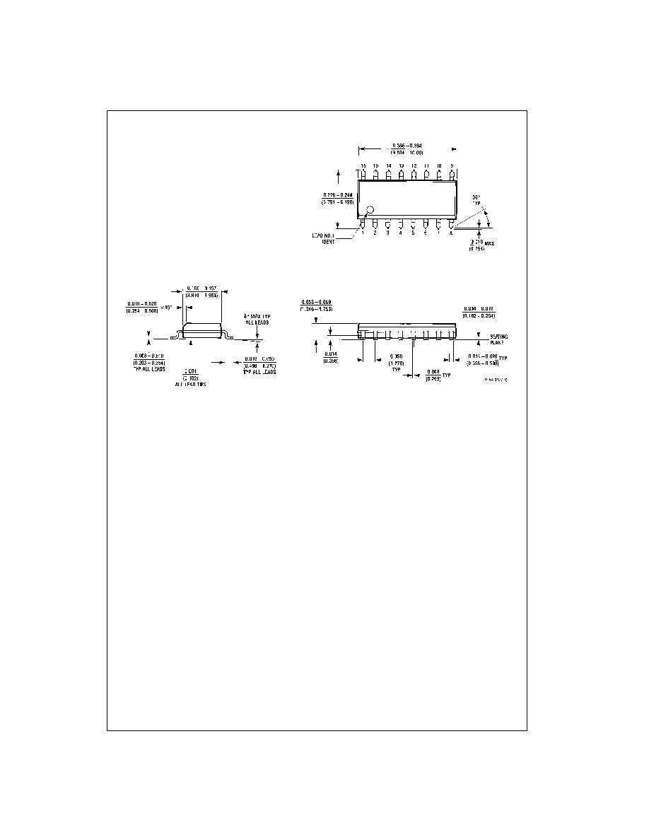
Physical Dimensions
inches (millimeters) unless otherwise noted
16-Lead Small Outline Integrated Circuit (SOIC), JEDEC MS-012, 0.150" Narrow
Package Number M16A