
October 1996
Revised March 1999
7
4
L
VX16
3
Low
V
o
l
t
a
ge Synchr
onous
Binar
y Count
er
wit
h
Sync
hronous
Clea
r
© 1999 Fairchild Semiconductor Corporation
DS012157.prf
www.fairchildsemi.com
74LVX163
Low Voltage Synchronous Binary Counter with
Synchronous Clear
General Description
The LVX163 is a synchronous modulo-16 binary counter.
This device is synchronously presettable for application in
programmable dividers and has two types of Count Enable
inputs plus a Terminal Count output for versatility in forming
multistage counters. The CLK input is active on the rising
edge. Both PE and MR inputs are active on low logic lev-
els. Presetting is synchronous to rising edge of the CLK
and the Clear function of the LVX163 is synchronous to the
CLK. Two enable inputs (CEP and CET) and Carry Output
are provided to enable easy cascading of counters, which
facilitates easy implementation of n-bit counters without
using external gates.
The inputs tolerate voltages up to 7V allowing the interface
of 5V systems to 3V systems.
Features
s
Input voltage level translation from 5V to 3V
s
Ideal for low power/low noise 3.3V applications
s
Guaranteed simultaneous switching noise and dynamic
threshold performance
Ordering Code:
Devices also available in Tape and Reel. Specify by appending the suffix letter "X" to the ordering code.
Logic Symbols
IEEE/IEC
Connection Diagram
Pin Descriptions
Order Number
Package Number
Package Description
74LVX163M
M16A
16-Lead Small Outline Integrated Circuit (SOIC), JEDEC MS-012, 0.150" Narrow
74LVX163SJ
M16D
16-Lead Small Outline Package (SOP), EIAJ TYPE II, 5.3mm Wide
74LVX163MTC
MTC16
16-Lead Thin Shrink Small Outline Package (TSSOP), JEDEC MO-153, 4.4mm Wide
Pin
Description
Names
CEP
Count Enable Parallel Input
CET
Count Enable Trickle Input
CP
Clock Pulse Input
MR
Synchronous Master Reset Input
P
0
≠P
3
Parallel Data Inputs
PE
Parallel Enable Inputs
Q
0
≠Q
3
Flip-Flop Outputs
TC
Terminal Count Output

www.fairchildsemi.com
2
74
L
VX163
Functional Description
The LVX163 counts in modulo-16 binary sequence. From
state 15 (HHHH) it increments to state 0 (LLLL). The clock
inputs of all flip-flops are driven in parallel through a clock
buffer. Thus all changes of the Q outputs occur as a result
of, and synchronous with, the LOW-to-HIGH transition of
the CP input signal. The circuits have four fundamental
modes of operation, in order of precedence: synchronous
reset, parallel load, count-up and hold. Four control
inputs--Synchronous Reset (MR), Parallel Enable (PE),
Count Enable Parallel (CEP) and Count Enable Trickle
(CET)--determine the mode of operation, as shown in the
Mode Select Table. A LOW signal on MR overrides count-
ing and parallel loading and allows all outputs to go LOW
on the next rising edge of CP. A LOW signal on PE over-
rides counting and allows information on the Parallel Data
(P
n
) inputs to be loaded into the flip-flops on the next rising
edge of CP. With PE and MR HIGH, CEP and CET permit
counting when both are HIGH. Conversely, a LOW signal
on either CEP or CET inhibits counting.
The LVX163 uses D-type edge-triggered flip-flops and
changing the MR, PE, CEP and CET inputs when the CP is
in either state does not cause errors, provided that the rec-
ommended setup and hold times, with respect to the rising
edge of CP, are observed.
The Terminal Count (TC) output is HIGH when CET is
HIGH and counter is in state 15. To implement synchro-
nous multistage counters, the TC outputs can be used with
the CEP and CET inputs in two different ways.
Figure 1 shows the connections for simple ripple carry, in
which the clock period must be longer than the CP to TC
delay of the first stage, plus the cumulative CET to TC
delays of the intermediate stages, plus the CET to CP
setup time of the last stage. This total delay plus setup time
sets the upper limit on clock frequency. For faster clock
rates, the carry lookahead connections shown in
Figure 2
are recommended. In this scheme the ripple delay through
the intermediate stages commences with the same clock
that causes the first stage to tick over from max to min in
the Up mode, or min to max in the Down mode, to start its
final cycle. Since this final cycle takes 16 clocks to com-
plete, there is plenty of time for the ripple to progress
through the intermediate stages. The critical timing that lim-
its the clock period is the CP to TC delay of the first stage
plus the CEP to CP setup time of the last stage. The TC
output is subject to decoding spikes due to internal race
conditions and is therefore not recommended for use as a
clock or asynchronous reset for flip-flops, registers or
counters. When the Parallel Enable (PE) is LOW, the paral-
lel data outputs O
0
≠O
3
are active and follow the flip-flop Q
outputs. A HIGH signal on PE forces O
0
≠O
3
to the High
impedance state but does not prevent counting, loading or
resetting.
Logic Equations: Count Enable
=
CEP ∑ CET ∑ PE
TC
=
Q
0
∑ Q
1
∑ Q
2
∑ Q
3
∑ CET
H
=
HIGH Voltage Level
L
=
LOW Voltage Level
X
=
Immaterial
=
LOW-to-HIGH Clock Transition
Mode Select Table
MR
PE
CET
CEP
Action on the Rising
Clock Edge (
)
L
X
X
X
Reset (Clear)
H
L
X
X
Load (P
n
Q
n
)
H
H
H
H
Count (Increment)
H
H
L
X
No Change (Hold)
H
H
X
L
No Change (Hold)

3
www.fairchildsemi.com
74
L
V
X
1
63
State Diagram
FIGURE 1.
FIGURE 2.
Block Diagram
Please note that this diagram is provided only for the understanding of logic operations and should not be used to estimate propagation delays.

www.fairchildsemi.com
4
74
L
VX163
Absolute Maximum Ratings
(Note 1)
Recommended Operating
Conditions
(Note 2)
Note 1: The "Absolute Maximum Ratings" are those values beyond which
the safety of the device cannot be guaranteed. The device should not be
operated at these limits. The parametric values defined in the Electrical
Characteristics tables are not guaranteed at the absolute maximum ratings.
The "Recommended Operating Conditions" table will define the conditions
for actual device operation.
Note 2: Unused inputs must be held HIGH or LOW. They may not float.
DC Electrical Characteristics
Noise Characteristics
Note 3: Parameter guaranteed by design.
Supply Voltage (V
CC
)
-
0.5V to
+
7.0V
DC Input Diode Current (I
IK
)
V
I
=
-
0.5V
-
20 mA
DC Input Voltage (V
I
)
-
0.5V to 7V
DC Output Diode Current (I
OK
)
V
O
=
-
0.5V
-
20 mA
V
O
=
V
CC
+
0.5V
+
20 mA
DC Output Voltage (V
O
)
-
0.5V to V
CC
+
0.5V
DC Output Source
or Sink Current (I
O
)
±
25 mA
DC V
CC
or Ground Current
(I
CC
or I
GND
)
±
50 mA
Storage Temperature (T
STG
)
-
65
∞
C to
+
150
∞
C
Power Dissipation
180 mW
Supply Voltage (V
CC
)
2.0V to 3.6V
Input Voltage (V
I
)
0V to 5.5V
Output Voltage (V
O
)
0V to V
CC
Operating Temperature (T
A
)
-
40
∞
C to
+
85
∞
C
Input Rise and Fall Time (
t/
v)
0 ns/V to 100 ns/V
Symbol
Parameter
V
CC
T
A
=
+
25
∞
C
T
A
=
-
40
∞
C to
+
85
∞
C
Units
Conditions
Min
Typ
Max
Min
Max
V
IH
HIGH Level Input
2.0
1.5
1.5
Voltage
3.0
2.0
2.0
V
3.6
2.4
2.4
V
IL
LOW Level Input
2.0
0.5
0.5
Voltage
3.0
0.8
0.8
V
3.6
0.8
0.8
V
OH
HIGH Level Output
2.0
1.9
2.0
1.9
V
IN
=
V
IL
or V
IH
I
OH
=
-
50
µ
A
Voltage
3.0
2.9
3.0
2.9
V
I
OH
=
-
50
µ
A
3.0
2.58
2.48
I
OH
=
-
4 mA
V
OL
LOW Level Output
2.0
0.0
0.1
0.1
V
IN
=
V
IL
or V
IH
I
OL
=
50
µ
A
Voltage
3.0
0.0
0.1
0.1
V
I
OL
=
50
µ
A
3.0
0.36
0.44
I
OL
=
4 mA
I
IN
Input Leakage Current
3.6
±
0.1
±
1.0
µ
A
V
IN
=
5.5V or GND
I
CC
Quiescent Supply Current
3.6
2.0
20.0
µ
A
V
IN
=
V
CC
or GND
Symbol
Parameter
V
CC
(V)
T
A
=
25
∞
C
Units
C
L
(pF)
Typ
Limits
V
OLP
Quiet Output Maximum
3.3
0.2
0.5
V
50
(Note 3)
Dynamic V
OL
V
OLV
Quiet Output Minimum
3.3
-
0.2
-
0.5
V
50
(Note 3)
Dynamic V
OL
V
IHD
Minimum HIGH Level
3.3
2.0
V
50
(Note 3)
Dynamic Input Voltage
V
ILD
Maximum LOW Level
3.3
0.8
V
50
(Note 3)
Dynamic Input Voltage
5
www.fairchildsemi.com
74
L
V
X
1
63
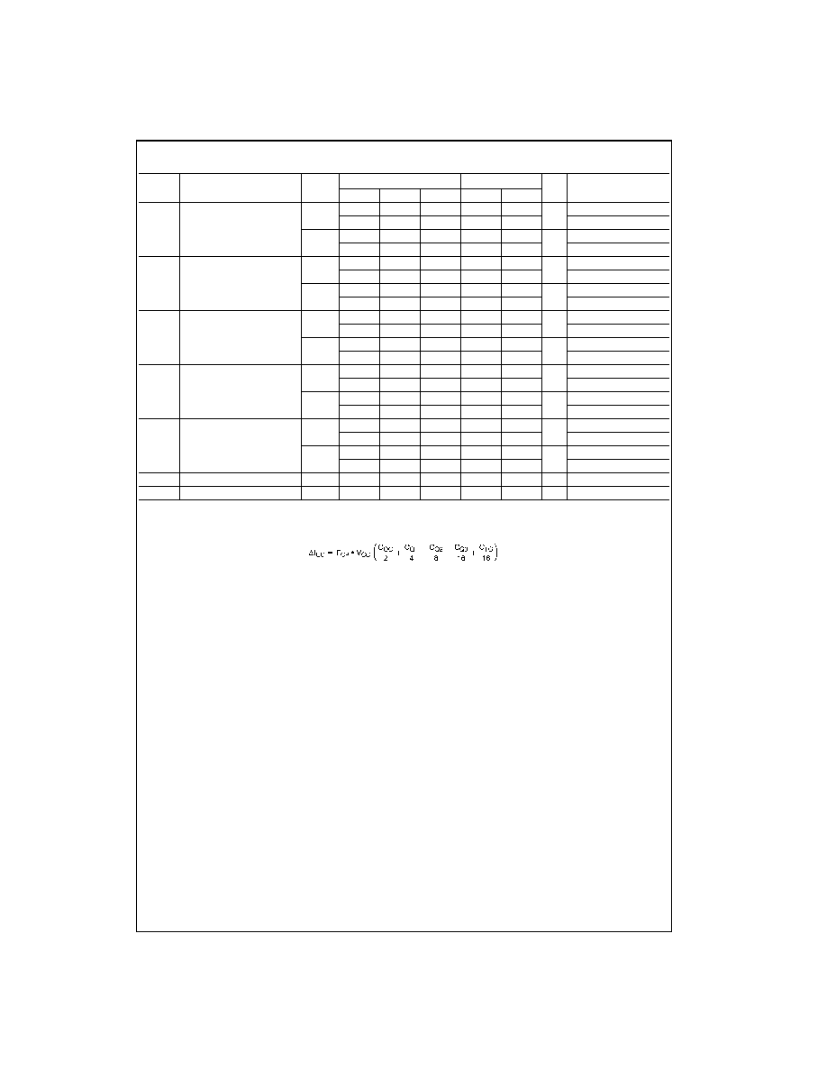
AC Electrical Characteristics
Note 4: C
PD
is defined as the value of the internal equivalent capacitance which is calculated from the operating current consumption without load. Average
operating current can be obtained by the equation: I
CC
(opr)
=
C
PD
* V
CC
* f
IN
+
I
CC
.
When the outputs drive a capacitive load, total current consumption is the sum of C
PD
, and
I
CC
which is obtained from the following formula:
C
Q0
≠C
Q3
and C
TC
are the capacitances at Q0≠Q3 and TC, respectively. F
CP
is the input frequency of the CP.
Symbol
Parameter
V
CC
(V)
T
A
=
25
∞
C
T
A
=
-
40
∞
C to
+
85
∞
C
Units
Conditions
Min
Typ
Max
Min
Max
t
PLH
Propagation Delay
2.7
9.0
14.0
1.0
16.0
ns
C
L
=
15 pF
t
PHL
Time (CP≠Q
n
)
11.3
17.0
1.0
19.0
C
L
=
50 pF
3.3
±
0.3
8.3
12.8
1.0
15.0
ns
C
L
=
15 pF
10.8
16.3
1.0
18.5
C
L
=
50 pF
t
PLH
Propagation Delay
2.7
9.5
14.3
1.0
16.7
ns
C
L
=
15 pF
t
PHL
Time (CP≠TC, Count)
12.5
18.5
1.0
20.5
C
L
=
50 pF
3.3
±
0.3
8.7
13.6
1.0
16.0
ns
C
L
=
15 pF
11.2
17.1
1.0
19.5
C
L
=
50 pF
t
PLH
Propagation Delay
2.7
11.4
18.0
1.0
21.0
ns
C
L
=
15 pF
t
PHL
Time (CP≠TC, Load)
14.0
21.0
1.0
24.0
C
L
=
50 pF
3.3
±
0.3
11.0
17.2
1.0
20.0
ns
C
L
=
15 pF
13.5
20.7
1.0
23.5
C
L
=
50 pF
t
PLH
Propagation Delay
2.7
8.6
13.5
1.0
15.0
ns
C
L
=
15 pF
t
PHL
Time (CET≠TC)
11.0
16.5
1.0
18.5
C
L
=
50 pF
3.3
±
0.3
7.5
12.3
1.0
14.5
ns
C
L
=
15 pF
10.5
15.8
1.0
18.0
C
L
=
50 pF
f
MAX
Maximum Clock
2.7
75
115
65
MHz
C
L
=
15 pF
Frequency
50
80
45
C
L
=
50 pF
3.3
±
0.3
80
130
70
MHz
C
L
=
15 pF
55
85
50
C
L
=
50 pF
C
IN
Input Capacitance
4
10
10
pF
V
CC
=
Open
C
PD
Power Dissipation Capacitance
23
pF
(Note 4)