
© 2003 Fairchild Semiconductor Corporation
DS011540
www.fairchildsemi.com
January 1993
Revised September 2003
7
4
L
VX42
45 8-
Bit
Dual
Sup
p
ly
T
r
ans
l
at
ing
T
r
an
sceive
r wi
th
3-
S
T
A
T
E Out
puts
74LVX4245
8-Bit Dual Supply Translating Transceiver
with 3-STATE Outputs
General Description
The LVX4245 is a dual-supply, 8-bit translating transceiver
that is designed to interface between a 5V bus and a 3V
bus in a mixed 3V/5V supply environment. The Transmit/
Receive (T/R) input determines the direction of data flow.
Transmit (active-HIGH) enables data from A Ports to B
Ports; Receive (active-LOW) enables data from B Ports to
A Ports. The Output Enable input, when HIGH, disables
both A and B Ports by placing them in a high impedance
condition. The A Port interfaces with the 5V bus; the B Port
interfaces with the 3V bus.
The LVX4245 is suitable for mixed voltage applications
such as laptop computers using 3.3V CPU's and 5V LCD
displays.
Features
s
Bidirectional interface between 5V and 3V buses
s
Control inputs compatible with TTL level
s
5V data flow at A Port and 3V data flow at B Port
s
Outputs source/sink 24 mA at 5V bus; 12 mA at 3V bus
s
Guaranteed simultaneous switching noise level and
dynamic threshold performance
s
Implements patented EMI reduction circuitry
s
Functionally compatible with the 74 series 245
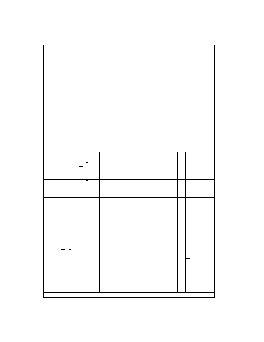
Ordering Code:
Devices also available in Tape and Reel. Specify by appending the suffix letter "X" to the ordering code.
Logic Symbol
Connection Diagram
Pin Descriptions
Truth Table
H
=
HIGH Voltage Level
L
=
LOW Voltage Level
X
=
Immaterial
Order Number
Package Number
Package Description
74LVX4245WM
M24B
24-Lead Small Outline Integrated Circuit (SOIC), JEDEC MS-013, 0.300" Wide
74LVX4245QSC
MQA24
24-Lead Quarter Size Outline Package (QSOP), JEDEC MO-137, 0.150" Wide
74LVX4245MTC
MTC24
24-Lead Thin Shrink Small Outline Package (TSSOP), JEDEC MO-153, 4.4mm Wide
Pin Names
Description
OE
Output Enable Input
T/R
Transmit/Receive Input
A
0
≠A
7
Side A Inputs or 3-STATE Outputs
B
0
≠B
7
Side B Inputs or 3-STATE Outputs
Inputs
Outputs
OE
T/R
L
L
Bus B Data to Bus A
L
H
Bus A Data to Bus B
H
X
HIGH-Z State

www.fairchildsemi.com
2
74L
VX4245
Logic Diagram
3
www.fairchildsemi.com
74
L
V
X
4
24
5
Absolute Maximum Ratings
(Note 1)
Recommended Operating
Conditions
(Note 2)
Note 1: The "Absolute Maximum Ratings" are those values beyond which
the safety of the device cannot be guaranteed. The device should not be
operated at these limits. The parametric values defined in the Electrical
Characteristics tables are not guaranteed at the absolute maximum ratings.
The "Recommended Operating Conditions" table will define the conditions
for actual device operation.
Note 2: Unused inputs must he held HIGH or LOW. They may not float.
DC Electrical Characteristics
Supply Voltage (V
CCA
, V
CCB
)
-
0.5V to
+
7.0V
DC Input Voltage (V
I
) @ OE, T/R
-
0.5V to V
CCA
+
0.5V
DC Input/Output Voltage (V
I/O
)
@ A
n
-
0.5V to V
CCA
+
0.5V
@B
n
-
0.5V to V
CCB
+
0.5V
DC Input Diode Current (I
IN
)
@ OE, T/R
±
20 mA
DC Output Diode Current (I
OK
)
±
50 mA
DC Output Source or Sink Current
(I
O
)
±
50 mA
DC V
CC
or Ground Current
per Output Pin (I
CC
or I
GND
)
±
50 mA
and Max Current @ I
CCA
±
200 mA
@ I
CCB
±
100 mA
Storage Temperature Range
(T
STG
)
-
65
∞
C to
+
150
∞
C
DC Latch-Up Source or
Sink Current
±
300 mA
Supply Voltage
V
CCA
4.5V to 5.5V
V
CCB
2.7V to 3.6V
Input Voltage (V
I
) @ OE, T/R
0V to V
CCA
Input/Output Voltage (V
I/O
)
@ A
n
0V to V
CCA
@ B
n
0V to V
CCB
Free Air Operating Temperature (T
A
)
-
40
∞
C to
+
85
∞
C
Minimum Input Edge Rate (
t/
V)
8 ns/V
V
IN
from 30% to 70% of V
CC
V
CC
@ 3.0V, 4.5V, 5.5V
Symbol
Parameter
V
CCA
V
CCB
T
A
+
25
∞
C
T
A
=
-
40
∞
C to
+
85
∞
C
Units
Conditions
(V)
(V)
Typ
Guaranteed Limits
V
IHA
Minimum
A
n
, T/R,
5.5
3.3
2.0
2.0
V
V
OUT
0.1V or
HIGH Level
OE
4.5
3.3
2.0
2.0
V
CC
-
0.1V
V
IHB
Input Voltage
B
n
5.0
3.6
2.0
2.0
5.0
2.7
2.0
2.0
V
ILA
Maximum
A
n
, T/R,
5.5
3.3
0.8
0.8
V
V
OUT
0.1V or
LOW Level
OE
4.5
3.3
0.8
0.8
V
CC
-
0.1V
V
ILB
Input Voltage
B
n
5.0
2.7
0.8
0.8
5.0
3.6
0.8
0.8
V
OHA
Minimum HIGH Level
4.5
3.0
4.5
4.4
4.4
V
I
OUT
=
-
100
µ
A
Output Voltage
4.5
3.0
4.25
3.86
3.76
I
OH
=
-
24 mA
V
OHB
4.5
3.0
2.99
2.9
2.9
V
I
OUT
=
-
100
µ
A
4.5
3.0
2.8
2.4
2.4
I
OH
=
-
12 mA
4.5
2.7
2.5
2.4
2.4
I
OL
=
-
8 mA
V
OLA
Maximum LOW Level
4.5
3.0
0.002
0.1
0.1
V
I
OUT
=
100
µ
A
Output Voltage
4.5
3.0
0.18
0.36
0.44
I
OL
=
24 mA
V
OLB
4.5
3.0
0.002
0.1
0.1
I
OUT
=
100
µ
A
4.5
3.0
0.1
0.31
0.4
V
I
OL
=
12 mA
4.5
2.7
0.1
0.31
0.4
I
OL
=
8 mA
I
IN
Maximum Input
V
I
=
V
CCA
, GND
Leakage Current
5.5
3.6
±
0.1
±
1.0
µ
A
@ OE, T/R
I
OZA
Maximum 3-STATE
V
I
=
V
IL
, V
IH
Output Leakage
5.5
3.6
±
0.5
±
5.0
µ
A
OE
=
V
CCA
@ A
n
V
O
=
V
CCA
, GND
I
OZB
Maximum 3-STATE
V
I
=
V
IL
, V
IH
Output Leakage
5.5
3.6
±
0.5
±
5.0
µ
A
OE
=
V
CCA
@ B
n
V
O
=
V
CCB
, GND
I
CC
Maximum I
CCT
/Input
5.5
3.6
1.0
1.35
1.5
mA
V
I
=
V
CCA
-
2.1V
@ A
n
, T/R, OE
Input @ B
n
5.5
3.6
0.35
0.5
mA
V
I
=
V
CCB
-
0.6V
www.fairchildsemi.com
4
74L
VX4245
DC Electrical Characteristics
(Continued)
Note 3: Maximum test duration 2.0 ms, one output loaded at a time.
Note 4: Worst case package.
Note 5: Max number of outputs defined as (n). Data inputs are driven 0V to V
CC
level; one output at GND.
Note 6: Max number of Data Inputs (n) switching. (n
-
1) inputs switching 0V to V
CC
level. Input-under-test switching:
V
CC
level to threshold (V
IHD
), OV to threshold (V
ILD
), f
=
1 MHz.
AC Electrical Characteristics
Note 7: Voltage Range 5.0V is 5.0V
±
0.5V.
Note 8: Voltage Range 3.3V is 3.3V
±
0.3V.
Note 9: Skew is defined as the absolute value of the difference between the actual propagation delay for any two separate outputs of the same device. The
specification applies to any outputs switching in the same direction, either HIGH-to-LOW (t
OSHL
) or LOW-to-HIGH (t
OSLH
). Parameter guaranteed by design.
Symbol
Parameter
V
CCA
V
CCB
T
A
+
25
∞
C
T
A
=
-
40
∞
C to
+
85
∞
C
Units
Conditions
(V)
(V)
Typ
Guaranteed Limits
I
CCA
Quiescent V
CCA
A
n
=
V
CCA
or GND
Supply Current
5.5
3.6
8
80
µ
A
B
n
=
V
CCB
or GND,
OE
=
GND T/R
=
GND
I
CCB
Quiescent V
CCB
A
n
=
V
CCA
or GND
Supply Current
5.5
3.6
5
50
µ
A
B
n
=
V
CCB
or GND,
OE
=
GND T/R
=
V
CCA
V
OLPA
Quiet Output Maximum
5.0
3.3
1.5
V
(Note 4)(Note 5)
V
OLPB
Dynamic V
OL
5.0
3.3
0.8
V
OLVA
Quiet Output Minimum
5.0
3.3
-
1.2
V
(Note 4)(Note 5)
V
OLVB
Dynamic V
OL
5.0
3.3
-
0.8
V
IHDA
Minimum HIGH Level
5.0
3.3
2.0
V
(Note 4)(Note 6)
V
IHDB
Dynamic Input Voltage
5.0
3.3
2.0
V
ILDA
Maximum LOW Level
5.0
3.3
0.8
V
(Note 4)(Note 6)
V
ILDB
Dynamic Input Voltage
5.0
3.3
0.8
Symbol
Parameters
T
A
=
+
25
∞
C
T
A
=
-
40
∞
C to
+
85
∞
C
T
A
=
-
40
∞
C to
+
85
∞
C
Units
C
L
=
50 pF
C
L
=
50 pF
C
L
=
50 pF
V
CCA
=
5V (Note 7)
V
CCA
=
5V (Note 7)
V
CCA
=
5V (Note 7)
V
CCB
=
3.3V (Note 8)
V
CCB
=
3.3V (Note 8)
V
CCB
=
2.7V
Min
Typ
Max
Min
Max
Min
Max
t
PHL
Propagation Delay
1.0
5.1
8.5
1.0
9.0
1.0
10.0
ns
t
PLH
A to B
1.0
5.3
8.5
1.0
9.0
1.0
10.0
t
PHL
Propagation Delay
1.0
5.4
8.5
1.0
9.0
1.0
10.0
ns
t
PLH
B to A
1.0
5.5
8.5
1.0
9.0
1.0
10.0
t
PZL
Output Enable Time
1.0
6.5
10.0
1.0
10.5
1.0
11.5
ns
t
PZH
OE to B
1.0
6.7
10.0
1.0
10.5
1.0
11.5
t
PZL
Output Enable Time
1.0
5.2
9.0
1.0
9.5
1.0
10.0
ns
t
PZH
OE to A
1.0
5.8
9.0
1.0
9.5
1.0
10.0
t
PHZ
Output Disable Time
1.0
6.0
9.5
1.0
10.0
1.0
10.0
ns
t
PLZ
OE to B
1.0
3.3
6.5
1.0
7.0
1.0
7.5
t
PHZ
Output Disable Time
1.0
3.9
7.0
1.0
7.5
1.0
7.5
ns
t
PLZ
OE to A
1.0
2.9
6.5
1.0
7.0
1.0
7.5
t
OSHL
Output to Output
t
OSLH
Skew (Note 9)
1.0
1.5
1.5
1.5
ns
Data to Output

5
www.fairchildsemi.com
74
L
V
X
4
24
5
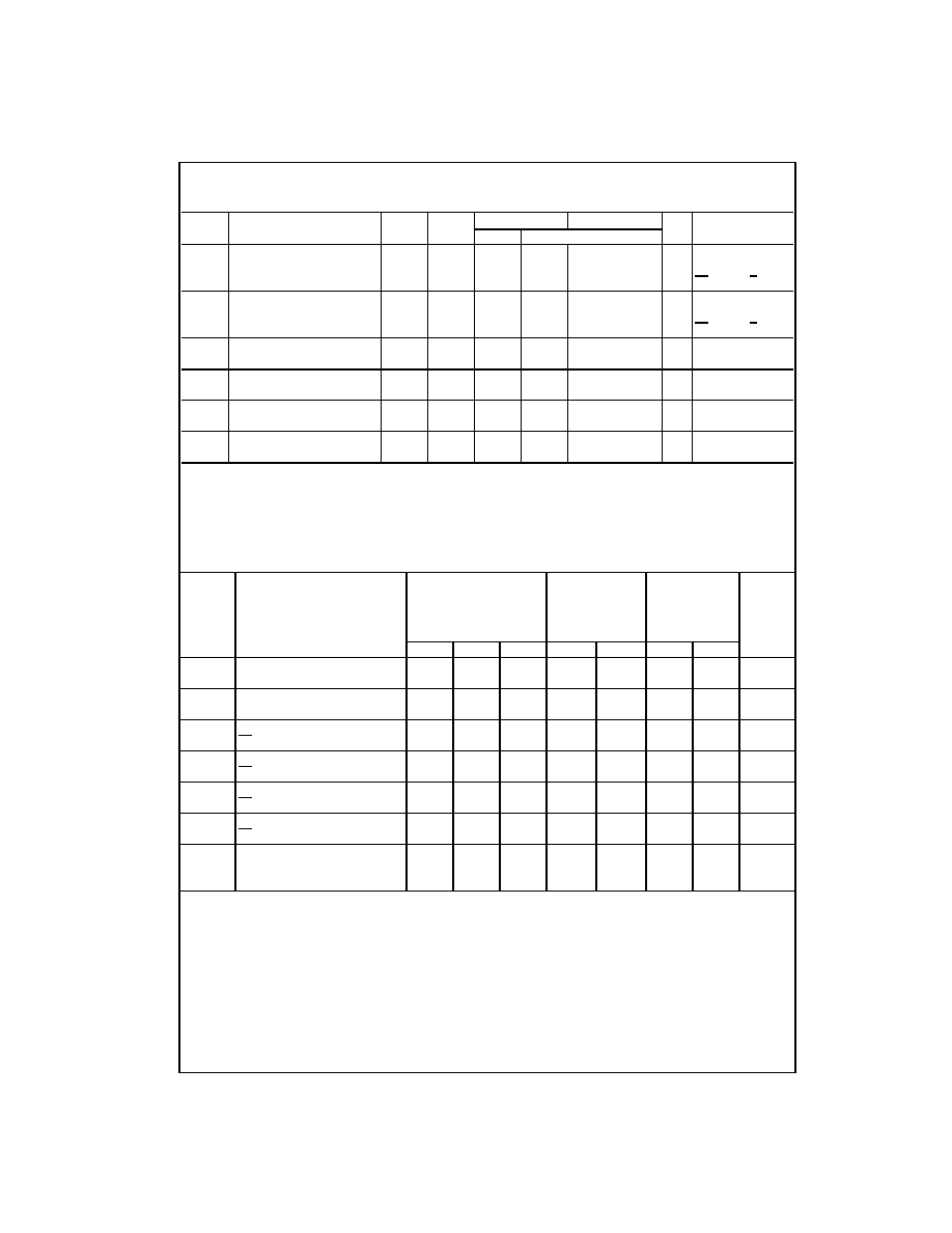
Capacitance
Note 10: C
PD
is measured at 10 MHz
8-Bit Dual Supply Translating Transceiver
The LVX4245 is a dual supply device capable of bidirec-
tional signal translation. This level shifting ability provides
an efficient interface between low voltage CPU local bus
with memory and a standard bus defined by 5V I/O levels.
The device control inputs can be controlled by either the
low voltage CPU and core logic or a bus arbitrator with 5V
I/O levels.
Manufactured on a sub-micron CMOS process, the
LVX4245 is ideal for mixed voltage applications such as
notebook computers using 3.3V CPU's and 5V peripheral
devices.
Power Up Considerations
To insure the system does not experience unnecessary I
CC
current draw, bus contention, or oscillations during power
up, the following guidelines should be adhered to (refer to
Table 1):
∑ Power up the control side of the device first. This is the
V
CCA
.
∑ OE should ramp with or ahead of V
CCA
. This will help
guard against bus contention.
∑ The Transmit/Receive control pin (T/R) should ramp with
or ahead of V
CCA
, this will ensure that the A Port data
pins are configured as inputs. With V
CCA
receiving
power first, the A I/O Port should be configured as inputs
to help guard against bus contention and oscillations.
∑ A side data inputs should be driven to a valid logic level.
This will prevent excessive current draw.
The above steps will ensure that no bus contention or oscil-
lations, and therefore no excessive current draw occurs
during the power up cycling of these devices. These steps
will help prevent possible damage to the translator devices
and potential damage to other system components.
TABLE 1. Low Voltage Translator Power Up Sequencing Table
Please reference Application Note AN-5001 for more detailed information on using Fairchild's LVX Low Voltage Dual
Supply CMOS Translating Transceivers.
Symbol
Parameter
Typ
Units
Conditions
C
IN
Input Capacitance
4.5
pF
V
CC
=
Open
C
I/O
Input/Output
15
pF
V
CCA
=
5.0V
Capacitance
V
CCB
=
3.3V
C
PD
Power Dissipation
B
A
55
pF
V
CCA
=
5.0V
Capacitance (Note 10)
A
B
40
pF
V
CCB
=
3.3V
Device Type
V
CCA
V
CCB
T/R
OE
A Side
I/O
B Side
I/O
Floatable Pin
Allowed
74LVX4245
5V
3V
ramp
ramp
logic
outputs
No
(power up 1st)
(power up 2nd)
with V
CCA
with V
CCA
0V or V
CCA