© 2005 Fairchild Semiconductor Corporation
DS011616
www.fairchildsemi.com
June 1993
Revised April 2005
7
4
L
VX57
3
Low V
o
l
t
age Oct
a
l Lat
ch
wi
th 3-ST
A
T
E
Out
put
s
74LVX573
Low Voltage Octal Latch with 3-STATE Outputs
General Description
The LVX573 is a high-speed octal latch with buffered com-
mon Latch Enable (LE) and buffered common Output
Enable (OE) inputs. The LVX573 is functionally identical to
the LVX373 but with inputs and outputs on opposite sides
of the package. The inputs tolerate up to 7V allowing inter-
face of 5V systems to 3V systems.
Features
s
Input voltage translation from 5V to 3V
s
Ideal for low power/low noise 3.3V applications
s
Guaranteed simultaneous switching noise level and
dynamic threshold performance
Ordering Code:
Devices also available in Tape and Reel. Specify by appending suffix letter "X" to the ordering code.
Pb-Free package per JEDEC J-STD-020B.
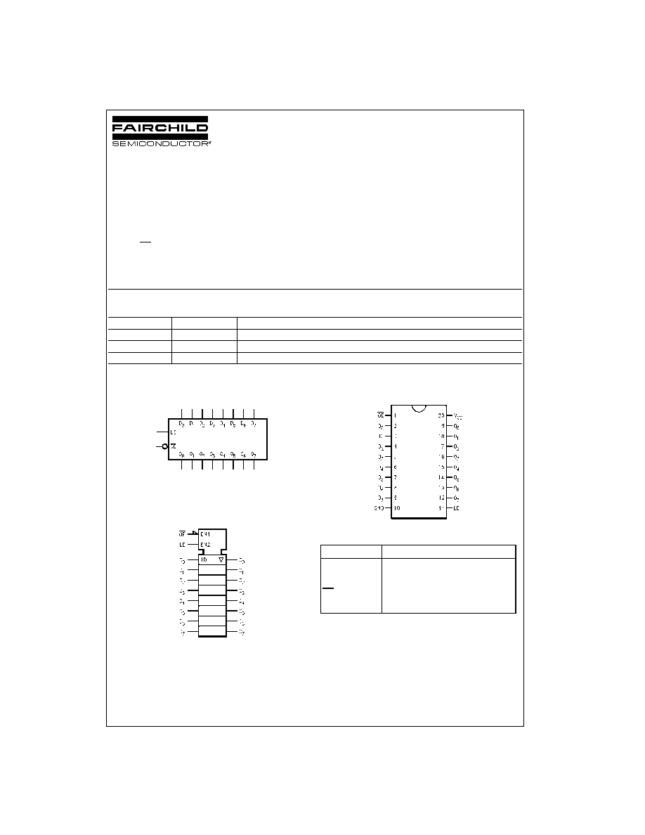
Logic Symbols
IEEE/IEC
Connection Diagram
Pin Descriptions
Order Number
Package Number
Package Description
74LVX573M
M20B
20-Lead Small Outline Integrated Circuit (SOIC), JEDEC MS-013, 0.300" Wide
74LVX573SJ
M20D
Pb-Free 20-Lead Small Outline Package (SOP), EIAJ TYPE II, 5.3mm Wide
74LVX573MTC
MTC20
20-Lead Thin Shrink Small Outline Package (TSSOP), JEDEC MO-153, 4.4mm Wide
Pin Names
Description
D
0
≠D
7
Data Inputs
LE
Latch Enable Input
OE
3-STATE Output Enable Input
O
0
≠O
7
3-STATE Latch Outputs
www.fairchildsemi.com
2
74
L
VX573
Functional Description
The LVX573 contains eight D-type latches. When the
enable (LE) input is HIGH, data on the D
n
inputs enters the
latches. In this condition the latches are transparent, i.e., a
latch output will change state each time its D input
changes. When LE is LOW the latches store the informa-
tion that was present on the D inputs a setup time preced-
ing the HIGH-to-LOW transition of LE. The 3-STATE
buffers are controlled by the Output Enable (OE) input.
When OE is LOW, the buffers are enabled. When OE is
HIGH the buffers are in the high impedance mode but this
does not interfere with entering new data into the latches.
Truth Table
H
HIGH Voltage
L
LOW Voltage
Z
High Impedance
X
Immaterial
O
0
Previous O
0
before HIGH-to-LOW transition of Latch Enable
Logic Diagram
Please note that this diagram is provided only for the understanding of logic operations and should not be used to estimate propagation delays.
Inputs
Outputs
OE
LE
D
O
n
L
H
H
H
L
H
L
L
L
L
X
O
0
H
X
X
Z
3
www.fairchildsemi.com
74
L
V
X
5
73
Absolute Maximum Ratings
(Note 1)
Recommended Operating
Conditions
(Note 2)
Note 1: The "Absolute Maximum Ratings" are those values beyond which
the safety of the device cannot be guaranteed. The device should not be
operated at these limits. The parametric values defined in the Electrical
Characteristics tables are not guaranteed at the absolute maximum ratings.
The "Recommended Operating Conditions" table will define the conditions
for actual device operation.
Note 2: Unused inputs must be held HIGH or LOW. They may not float.
DC Electrical Characteristics
Noise Characteristics
(Note 3)
Note 3: (Input t
r
t
f
3ns)
Supply Voltage (V
CC
)
0.5V to
7.0V
DC Input Diode Current (I
IK
)
V
I
0.5V
20 mA
DC Input Voltage (V
I
)
0.5V to 7V
DC Output Diode Current (I
OK
)
V
O
0.5V
20 mA
V
O
V
CC
0.5V
20 mA
DC Output Voltage (V
O
)
0.5V to V
CC
0.5V
DC Output Source
or Sink Current (I
O
)
r
25 mA
DC V
CC
or Ground Current
(I
CC
or I
GND
)
r
75 mA
Storage Temperature (T
STG
)
65
q
C to
150
q
C
Power Dissipation
180 mW
Supply Voltage (V
CC
)
2.0V to 3.6V
Input Voltage (V
I
)
0V to 5.5V
Output Voltage (V
O
)
0V to V
CC
Operating Temperature (T
A
)
40
q
C to
85
q
C
Input Rise and Fall Time (
'
t/
'
V)
0 ns/V to 100 ns/V
Symbol
Parameter
V
CC
T
A
25
q
C
T
A
40
q
C to
85
q
C
Units
Conditions
Min
Typ
Max
Min
Max
V
IH
HIGH Level
2.0
1.5
1.5
Input Voltage
3.0
2.0
2.0
V
3.6
2.4
2.4
V
IL
LOW Level
2.0
0.5
0.5
Input Voltage
3.0
0.8
0.8
V
3.6
0.8
0.8
V
OH
HIGH Level
2.0
1.9
2.0
1.9
V
IN
V
IH
or V
IL
I
OH
50
P
A
Output Voltage
3.0
2.9
3.0
2.9
V
I
OH
50
P
A
3.0
2.58
2.48
I
OH
4 mA
V
OL
LOW Level
2.0
0.0
0.1
0.1
V
IN
V
IH
or V
IL
I
OL
50
P
A
Output Voltage
3.0
0.0
0.1
0.1
V
I
OL
50
P
A
3.0
0.36
0.44
I
OL
4 mA
I
OZ
3-STATE Output
3.6
r
0.25
r
2.5
P
A
V
IN
V
IH
or V
IL
Off-State Current
V
OUT
V
CC
or GND
I
IN
Input Leakage Current
3.6
r
0.1
r
1.0
P
A
V
IN
5.5V or GND
I
CC
Quiescent Supply Current
3.6
4.0
40.0
P
A
V
IN
V
CC
or GND
Symbol
Parameter
V
CC
T
A
25
q
C
Units
C
L
(pF)
(V)
Typ
Limit
V
OLP
Quiet Output Maximum Dynamic V
OL
3.3
0.5
0.8
V
50
V
OLV
Quiet Output Minimum Dynamic V
OL
3.3
0.5
0.8
V
50
V
IHD
Minimum HIGH Level Dynamic Input Voltage
3.3
2.0
V
50
V
ILD
Maximum LOW Level Dynamic Input Voltage
3.3
0.8
V
50
www.fairchildsemi.com
4
74
L
VX573
AC Electrical Characteristics
Note 4: Parameter guaranteed by design. t
OSLH
|t
PLHm
t
PLHn
|, t
OSHL
|t
PHLm
t
PHLn
|.
Capacitance
Note 5: C
PD
is defined as the value of the internal equivalent capacitance which is calculated from the operating current consumption without load.
Symbol
Parameter
V
CC
T
A
25
q
C
T
A
40
q
C to
85
q
C
Units
Conditions
(V)
Min
Typ
Max
Min
Max
t
PLH
Propagation
2.7
7.6
14.5
1.0
17.5
ns
C
L
15 pF
t
PHL
Delay Time
10.1
18.0
1.0
21.0
C
L
50 pF
D
n
to O
n
3.3
r
0.3
5.9
9.3
1.0
11.0
C
L
15 pF
8.4
12.8
1.0
14.5
C
L
50 pF
t
PLH
Propagation
2.7
8.2
15.6
1.0
18.5
ns
C
L
15 pF
t
PHL
Delay Time
10.7
19.1
1.0
22.0
C
L
50 pF
LE to O
n
3.3
r
0.3
6.4
10.1
1.0
12.0
C
L
15 pF
8.9
13.6
1.0
15.5
C
L
50 pF
t
PZL
3-STATE Output
2.7
7.8
15.0
1.0
18.5
ns
C
L
15 pF, R
L
1 k
:
t
PZH
Enable Time
10.3
18.5
1.0
22.0
C
L
50 pF, R
L
1 k
:
3.3
r
0.3
6.1
9.7
1.0
12.0
C
L
15 pF, R
L
1 k
:
8.6
13.2
1.0
15.5
C
L
50 pF, R
L
1 k
:
t
PLZ
3-STATE Output
2.7
12.1
19.1
1.0
22.0
ns
C
L
50 pF, R
L
1 k
:
t
PHZ
Disable Time
3.3
r
0.3
10.1
13.6
1.0
15.5
C
L
50 pF, R
L
1 k
:
t
W
LE Pulse
2.7
6.5
7.5
ns
Width
3.3
r
0.3
5.0
5.0
t
S
Setup Time
2.7
5.0
5.0
ns
D
n
to LE
3.3
r
0.3
3.5
3.5
t
H
Hold Time
2.7
1.5
1.5
ns
D
n
to LE
3.3
r
0.3
1.5
1.5
t
OSHL
Output to Output
2.7
1.5
1.5
ns
C
L
50 pF
t
OSLH
Skew (Note 4)
2.3
1.5
1.5
Symbol
Parameter
T
A
25
q
C
T
A
40
q
C to
85
q
C
Units
Min
Typ
Max
Min
Max
C
IN
Input Capacitance
4
10
10
pF
C
OUT
Output Capacitance
6
pF
C
PD
Power Dissipation
27
pF
Capacitance (Note 5)
5
www.fairchildsemi.com
74
L
V
X
5
73
Physical Dimensions
inches (millimeters) unless otherwise noted
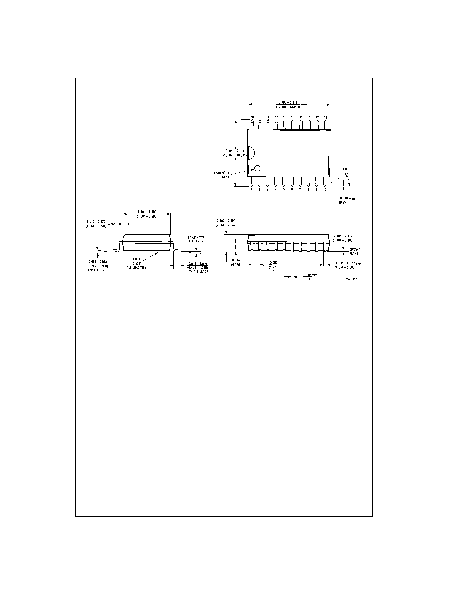
20-Lead Small Outline Integrated Circuit (SOIC), JEDEC MS-013, 0.300" Wide
Package Number M20B