 | –≠–ª–µ–∫—Ç—Ä–æ–Ω–Ω—ã–π –∫–æ–º–ø–æ–Ω–µ–Ω—Ç: 74LVX574 | –°–∫–∞—á–∞—Ç—å:  PDF PDF  ZIP ZIP |
June 1993
Revised March 1999
7
4
L
VX57
4
Low V
o
l
t
a
ge
Oct
a
l D-T
ype Fli
p
-
F
lop wit
h
3-
ST
A
T
E Output
s
© 1999 Fairchild Semiconductor Corporation
DS500050.prf
www.fairchildsemi.com
74LVX574
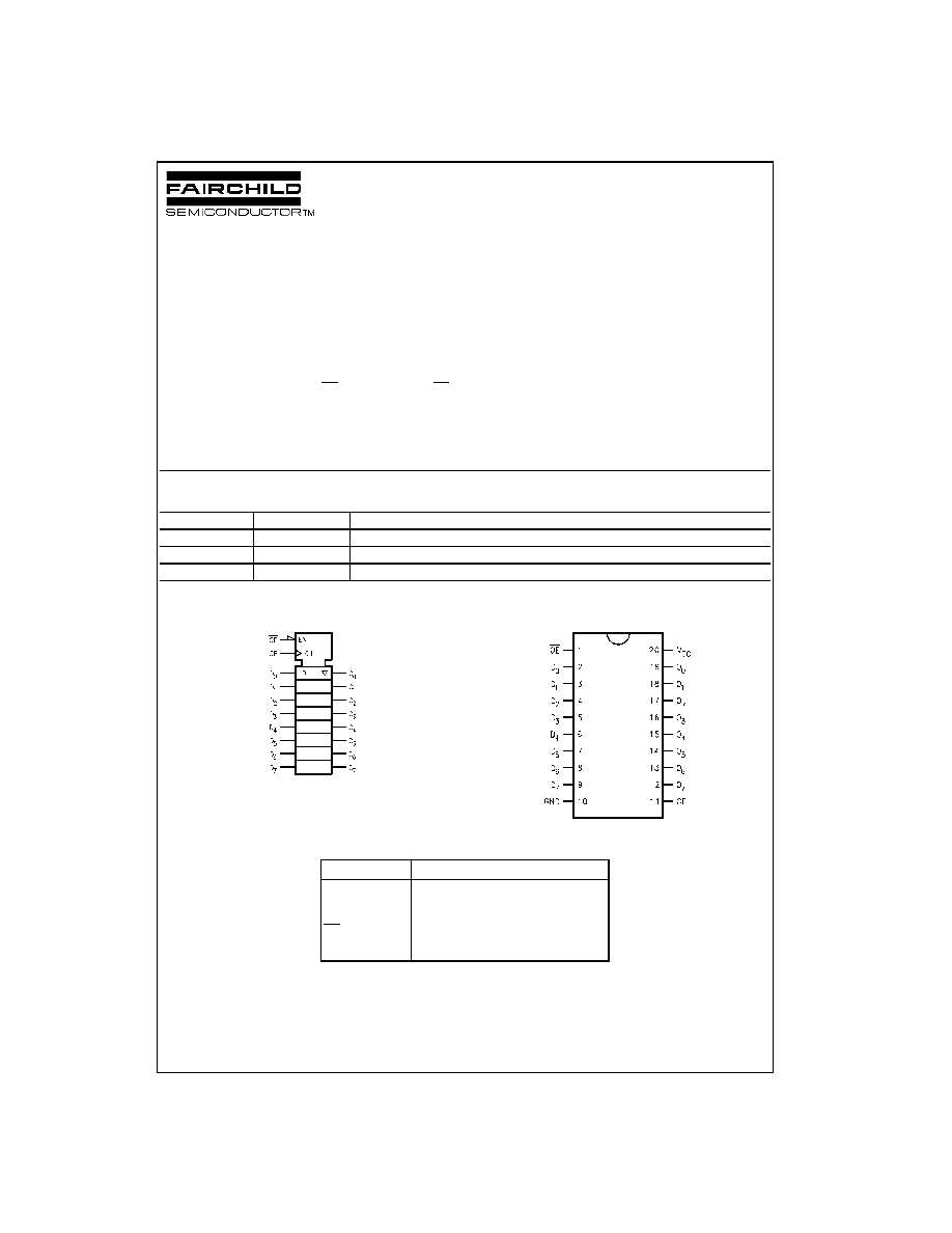
Low Voltage Octal D-Type Flip-Flop with
3-STATE Outputs
General Description
The LVX574 is a high-speed octal D-type flip-flop which is
controlled by an edge-triggered clock input (CP) and a buff-
ered common Output Enable (OE) input. When the OE
input is HIGH, the eight outputs are in a high impedance
state. The LVX574 is functionally identical to the LVX374
but with inputs and outputs on opposite sides of the pack-
age. The inputs tolerate up to 7V allowing interface of 5V
systems to 3V systems.
Features
s
Input voltage translation from 5V to 3V
s
Ideal for low power/low noise 3.3V applications
s
Guaranteed simultaneous switching noise level and
dynamic threshold performance
Ordering Code:
Devices also available in Tape and Reel. Specify by appending the suffix letter "X" to the ordering code.
Logic Symbol
Connection Diagram
Pin Descriptions
Order Number
Package Number
Package Description
74LVX574M
M20B
20-Lead Small Outline Integrated Circuit (SOIC), JEDEC MS-013, 0.300" Wide
74LVX574SJ
M20D
20-Lead Small Outline Package (SOP), EIAJ TYPE II, 5.3mm Wide
74LVX574MTC
MTC20
20-Lead Thin Shrink Small Outline Package (TSSOP), JEDEC MO-153, 4.4mm Wide
Pin Names
Description
D
0
≠D
7
Data Inputs
CP
Clock Pulse Input
OE
3-STATE Output Enable Input
O
0
≠O
7
3-STATE Outputs
www.fairchildsemi.com
2
74
L
VX574
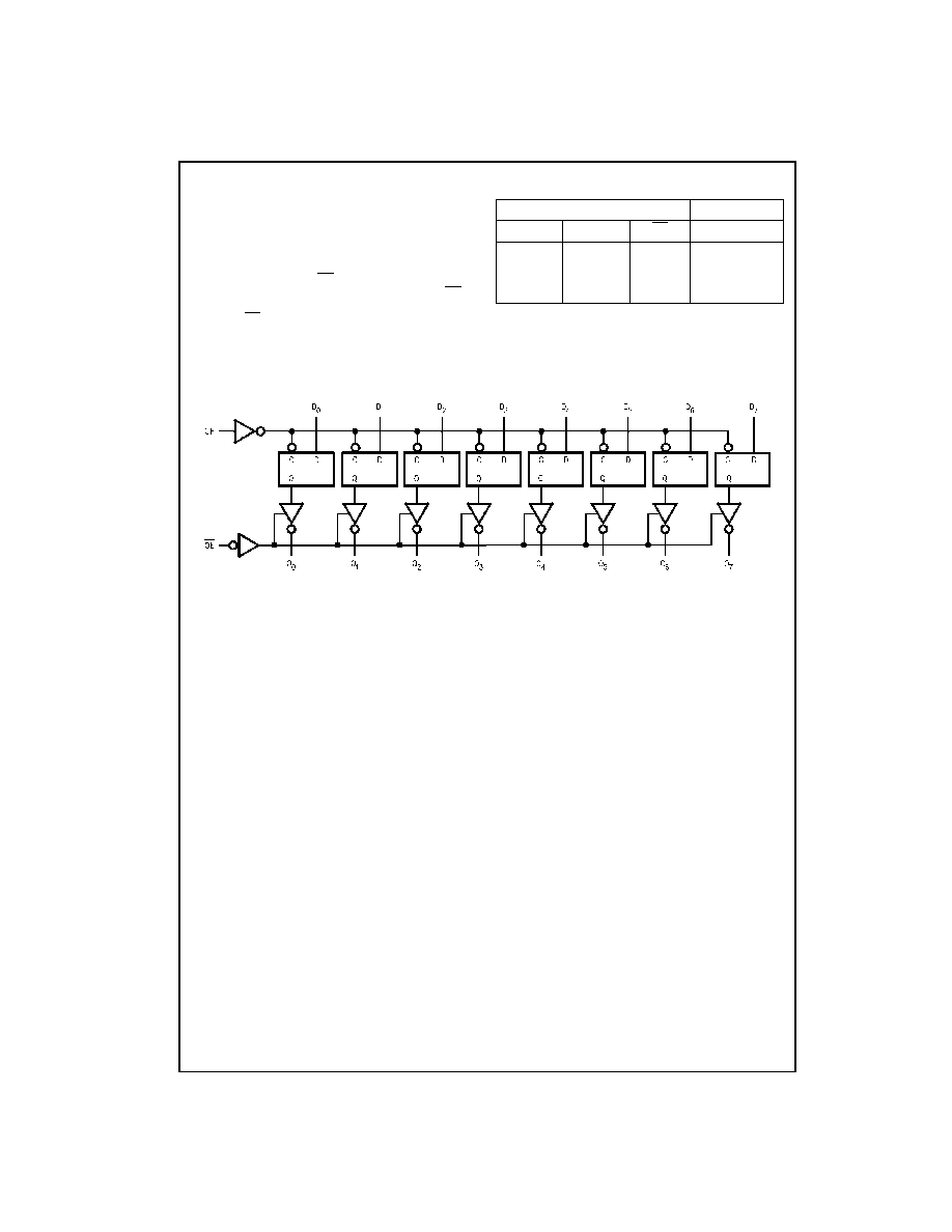
Functional Description
The LVX574 consists of eight edge-triggered flip-flops with
individual D-type inputs and 3-STATE true outputs. The
buffered clock and buffered Output Enable are common to
all flip-flops. The eight flip-flops will store the state of their
individual D inputs that meet the setup and hold time
requirements on the LOW-to-HIGH Clock (CP) transition.
With the Output Enable (OE) LOW, the contents of the
eight flip-flops are available at the outputs. When the OE is
HIGH, the outputs go to the high impedance state. Opera-
tion of the OE input does not affect the state of the flip-
flops.
Truth Table
H
=
HIGH Voltage Level
L
=
LOW Voltage Level
X
=
Immaterial
Z
=
High Impedance
=
LOW-to-HIGH Transition
Logic Diagram
Please note that this diagram is provided only for the understanding of logic operations and should not be used to estimate propagation delays.
Inputs
Outputs
D
n
CP
OE
O
n
H
L
H
L
L
L
X
X
H
Z
3
www.fairchildsemi.com
74
L
V
X
5
74
Absolute Maximum Ratings
(Note 1)
Recommended Operating
Conditions
(Note 2)
Note 1: The "Absolute Maximum Ratings" are those values beyond which
the safety of the device cannot be guaranteed. The device should not be
operated at these limits. The parametric values defined in the Electrical
Characteristics tables are not guaranteed at the absolute maximum ratings.
The "Recommended Operating Conditions" table will define the conditions
for actual device operation.
Note 2: Unused inputs must be held HIGH or LOW. They may not float.
DC Electrical Characteristics
Noise Characteristics
(Note 3)
Note 3: (Input t
r
=
t
f
=
3 ns)
Supply Voltage (V
CC
)
-
0.5V to
+
7.0V
DC Input Diode Current (I
IK
)
V
I
=
-
0.5V
-
20 mA
DC Input Voltage (V
I
)
-
0.5V to 7V
DC Output Diode Current (I
OK
)
V
O
=
-
0.5V
-
20 mA
V
O
=
V
CC
+
0.5V
+
20 mA
DC Output Voltage (V
O
)
-
0.5V to V
CC
+
0.5V
DC Output Source
or Sink Current (I
O
)
±
25 mA
DC V
CC
or Ground Current
(I
CC
or I
GND
)
±
75 mA
Storage Temperature (T
STG
)
-
65
∞
C to
+
150
∞
C
Power Dissipation
180 mW
Supply Voltage (V
CC
)
2.0V to 3.6V
Input Voltage (V
I
)
0V to 5.5V
Output Voltage (V
O
)
0V to V
CC
Operating Temperature (T
A
)
-
40
∞
C to
+
85
∞
C
Input Rise and Fall Time (
t/
V)
0 ns/V to 100 ns/V
Symbol
Parameter
V
CC
T
A
=
+
25
∞
C
T
A
=
-
40
∞
C to
+
85
∞
C
Units
Conditions
Min
Typ
Max
Min
Max
V
IH
HIGH Level
2.0
1.5
1.5
Input Voltage
3.0
2.0
2.0
V
3.6
2.4
2.4
V
IL
LOW Level
2.0
0.5
0.5
Input Voltage
3.0
0.8
0.8
V
3.6
0.8
0.8
V
OH
HIGH Level
2.0
1.9
2.0
1.9
V
IN
=
V
IH
or V
IL
I
OH
=
-
50
µ
A
Output Voltage
3.0
2.9
3.0
2.9
V
I
OH
=
-
50
µ
A
3.0
2.58
2.48
I
OH
=
-
4 mA
V
OL
LOW Level
2.0
0.0
0.1
0.1
V
IN
=
V
IH
or V
IL
I
OL
=
50
µ
A
Output Voltage
3.0
0.0
0.1
0.1
V
I
OL
=
50
µ
A
3.0
0.36
0.44
I
OL
=
4 mA
I
OZ
3-STATE Output
3.6
±
0.25
±
2.5
µ
A
V
IN
=
V
IH
or V
IL
Off-State Current
V
OUT
=
V
CC
or GND
I
IN
Input Leakage Current
3.6
±
0.1
±
1.0
µ
A
V
IN
=
5.5V or GND
I
CC
Quiescent Supply Current
3.6
4.0
40.0
µ
A
V
IN
=
V
CC
or GND
Symbol
Parameter
V
CC
(V)
T
A
=
25
∞
C
Units
C
L
(pF)
Typ
Limit
V
OLP
Quiet Output Maximum Dynamic V
OL
3.3
0.5
0.8
V
50
V
OLV
Quiet Output Minimum Dynamic V
OL
3.3
-
0.5
-
0.8
V
50
V
IHD
Minimum HIGH Level Dynamic Input Voltage
3.3
2.0
V
50
V
ILD
Maximum LOW Level Dynamic Input Voltage
3.3
0.8
V
50

www.fairchildsemi.com
4
74
L
VX574
AC Electrical Characteristics
(Note 4)
Note 4: Parameter guaranteed by design. t
OSLH
=
|t
PLHm
-
t
PLHn
|, t
OSHL
=
|t
PHLm
-
t
PHLn
|.
Capacitance
Note 5: C
PD
is defined as the value of the internal equivalent capacitance which is calculated from the operating current consumption without load.
Symbol
Parameter
V
CC
(V)
T
A
=
+
25
∞
C
T
A
=
-
40
∞
C to
+
85
∞
C
Units
Conditions
Min
Typ
Max
Min
Max
f
MAX
Maximum
2.7
60
115
50
MHZ
C
L
=
15 pF
Clock
45
60
40
C
L
=
50 pF
Frequency
3.3
±
0.3
80
125
65
C
L
=
15 pF
50
75
45
C
L
=
50 pF
t
PLH
Propagation
2.7
9.2
14.5
1.0
17.5
ns
C
L
=
15 pF
t
PHL
Delay Time
11.5
18.0
1.0
21.0
C
L
=
50 pF
CP to O
n
3.3
±
0.3
8.5
13.2
1.0
15.5
C
L
=
15 pF
11.0
16.7
1.0
19.0
C
L
=
50 pF
t
PZL
3-STATE Output
2.7
9.8
15.0
1.0
18.5
ns
C
L
=
15 pF, R
L
=
1 k
t
PZH
Enable Time
11.4
18.5
1.0
22.0
C
L
=
50 pF, R
L
=
1 k
3.3
±
0.3
8.2
12.8
1.0
15.0
C
L
=
15 pF, R
L
=
1 k
10.7
16.3
1.0
18.5
C
L
=
50 pF, R
L
=
1 k
t
PLZ
t
PHZ
3-STATE Output
2.7
12.1
19.1
1.0
22.0
ns
C
L
=
50 pF, R
L
=
1 k
Disable Time
3.3
±
0.3
11.0
15.0
1.0
17.0
C
L
=
50 pF, R
L
=
1 k
t
W
CP Pulse
2.7
6.5
7.5
ns
Width
3.3
±
0.3
5.0
5.0
t
S
Setup Time
2.7
5.0
5.0
ns
D
n
to CP
3.3
±
0.3
3.5
3.5
t
H
Hold Time
2.7
1.5
1.5
ns
D
n
to CP
3.3
±
0.3
1.5
1.5
t
OSHL
Output to Output
2.7
1.5
1.5
ns
C
L
=
50 pF
t
OSLH
Skew (Note 4)
3.3
1.5
1.5
Symbol
Parameter
T
A
=
+
25
∞
C
T
A
=
-
40
∞
C to
+
85
∞
C
Units
Min
Typ
Max
Min
Max
C
IN
Input Capacitance
4
10
10
pF
C
OUT
Output Capacitance
6
pF
C
PD
Power Dissipation
27
pF
Capacitance
(Note 5)

5
www.fairchildsemi.com
74
L
V
X
5
74
Physical Dimensions
inches (millimeters) unless otherwise noted
20-Lead Small Outline Integrated Circuit (SOIC), JEDEC MS-013, 0.300" Wide
Package Number M20B
20-Lead Small Outline Package (SOP), EIAJ TYPE II, 5.3mm Wide
Package Number M20D