 | –≠–ª–µ–∫—Ç—Ä–æ–Ω–Ω—ã–π –∫–æ–º–ø–æ–Ω–µ–Ω—Ç: 74MMC221N | –°–∫–∞—á–∞—Ç—å:  PDF PDF  ZIP ZIP |

November 1987
Revised January 1999
MM74C221 Dual Monosta
b
l
e M
u
lt
ivi
b
rat
o
r
© 1999 Fairchild Semiconductor Corporation
DS005904.prf
www.fairchildsemi.com
MM74C221
Dual Monostable Multivibrator
General Description
The MM74C221 dual monostable multivibrator is a mono-
lithic complementary MOS integrated circuit. Each multivi-
brator features a negative-transition-triggered input and a
positive-transition-triggered input, either of which can be
used as an inhibit input, and a clear input.
Once fired, the output pulses are independent of further
transitions of the A and B inputs and are a function of the
external timing components C
EXT
and R
EXT
. The pulse
width is stable over a wide range of temperature and V
CC
.
Pulse stability will be limited by the accuracy of external
timing components. The pulse width is approximately
defined by the relationship t
W(OUT)
C
EXT
R
EXT
. For fur-
ther information and applications, see AN-138.
Features
s
Wide supply voltage range:
4.5V to 15V
s
Guaranteed noise margin:
1.0V
s
High noise immunity:
0.45 V
CC
(typ.)
s
Low power TTL compatibility:
fan out of 2 driving 74L
Ordering Code:
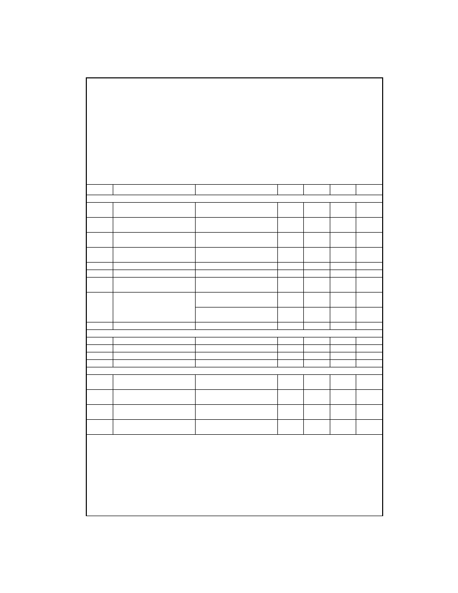
Connection Diagrams
Timing Component
Pin Assignments for DIP
Top View
Truth Table
H
=
HIGH Level
�
=
One HIGH level pulse
L
=
LOW Level
=
One LOW level pulse
=
Transition from LOW-to-HIGH
X
=
Irrelevant
=
Transition from HIGH-to-LOW
Order Number
Package Number
Package Description
74MMC221N
N16E
16-Lead Plastic Dual-in-Line Package (PDIP), JEDEC MS-001, 0.300" Wide
Inputs
Outputs
Clear
A
B
Q
Q
L
X
X
L
H
X
H
X
L
H
X
X
L
L
H
H
L
�
H
H
�
www.fairchildsemi.com
2
M
M
74C221
Absolute Maximum Ratings
(Note 1)
Note 1: "Absolute Maximum Ratings" are those values beyond which the
safety of the device cannot be guaranteed. Except for "Operating Tempera-
ture Range" they are not meant to imply that the devices should be oper-
ated at these limits. The Electrical Characteristics table provides conditions
for actual device operation.
DC Electrical Characteristics
Max/min limits apply across temperature range, unless otherwise noted
Note 2: In Standby (Q
=
Logic "0") the power dissipated equals the leakage current plus V
CC
/R
EXT
.
Voltage at Any Pin
-
0.3V to V
CC
+
0.3V
Operating Temperature Range
-
40
∞
C to
+
85
∞
C
Storage Temperature Range
-
65
∞
C to
+
150
∞
C
Power Dissipation
Dual-In-Line
700 mW
Small Outline
500 mW
Operating V
CC
Range
4.5V to 15V
Absolute Maximum V
CC
18V
R
EXT
80 V
CC
(
)
Lead Temperature
(Soldering, 10 seconds)
260
∞
C
Symbol
Parameter
Conditions
Min
Typ
Max
Units
CMOS to CMOS
V
IN(1)
Logical "1" Input Voltage
V
CC
=
5V
3.5
V
V
CC
=
10V
8.0
V
V
IN(0)
Logical "0" Input Voltage
V
CC
=
5V
1.5
V
V
CC
=
10V
2.0
V
V
OUT(1)
Logical "1" Output Voltage
V
CC
=
5V, I
O
=
-
10
µ
A 4.5
V
V
CC
=
10V, I
O
=
-
10
µ
A
9.0
V
V
OUT(0)
Logical "0" Output Voltage
V
CC
=
5V, I
O
=
+
10
µ
A
0.5
V
V
CC
=
10V, I
O
=
+
10
µ
A
1
V
I
IN(1)
Logical "1" Input Current
V
CC
=
15V, V
IN
=
15V
0.005
1.0
µ
A
I
IN(0)
Logical "0" Input Current
V
CC
=
15V, V
IN
=
0V
-
1.0
-
0.005
µ
A
I
CC
Supply Current (Standby)
V
CC
=
15V, R
EXT
=
,
0.05
300
µ
A
Q1, Q2
=
Logic "0" (Note 2)
I
CC
Supply Current
V
CC
=
15V, Q1
=
Logic "1",
15
mA
(During Output Pulse)
Q2
=
Logic "0" (Figure 4)
V
CC
=
5V, Q1
=
Logic "1",
2
mA
Q2
=
Logic "0" (Figure 4)
Leakage Current at R/C
EXT
Pin
V
CC
=
15V, V
CEXT
=
5V
0.01
3.0
µ
A
CMOS/LPTTL Interface
V
IN(1)
Logical "1" Input Voltage
V
CC
=
4.75V
V
CC
-
1.5
V
V
IN(0)
Logical "0" Input Voltage
V
CC
=
4.75V
0.8
V
V
OUT(1)
Logical "1" Output Voltage
V
CC
=
4.75V, I
O
=
-
360
µ
A
2.4
V
V
OUT(0)
Logical "0" Output Voltage
V
CC
=
4.75V, I
O
=
360
µ
A
0.4
V
Output Drive (See Family Characteristics Data Sheet) (Short Circuit Current)
I
SOURCE
Output Source Current
V
CC
=
5V
-
1.75
mA
(P-Channel)
T
A
=
25
∞
C, V
OUT
=
0V
I
SOURCE
Output Source Current
V
CC
=
10V
-
8
mA
(P-Channel)
T
A
=
25
∞
C, V
OUT
=
0V
I
SINK
Output Sink Current
V
CC
=
5V
1.75
mA
(N-Channel)
T
A
=
25
∞
C, V
OUT
=
V
CC
I
SINK
Output Sink Current
V
CC
=
10V
8
mA
(N-Channel)
T
A
=
25
∞
C, V
OUT
=
V
CC
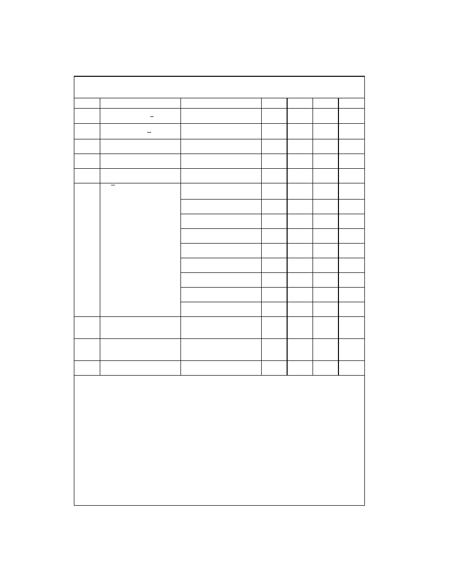
3
www.fairchildsemi.com
MM74C221
AC Electrical Characteristics
(Note 3)
T
A
=
25
∞
C, C
L
=
50 pF, unless otherwise noted
Note 3: AC Parameters are guaranteed by DC correlated testing.
Note 4: See AN-138 for detailed explanation R
ON
.
Note 5: Maximum output duty cycle
=
R
EXT
/R
EXT
+
1000.
Note 6: Capacitance is guaranteed by periodic testing.
Symbol
Parameter
Conditions
Min
Typ
Max
Units
t
pd A, B
Propagation Delay from Trigger
V
CC
=
5V
250
500
ns
Input (A, B) to Output Q, Q
V
CC
=
10V
120
250
ns
t
pd CL
Propagation Delay from Clear
V
CC
=
5V
250
500
ns
Input (CL) to Output Q, Q
V
CC
=
10V
120
250
ns
t
S
Time Prior to Trigger Input (A, B)
V
CC
=
5V
150
50
ns
that Clear must be Set
V
CC
=
10V
60
20
ns
t
W(A, B)
Trigger Input (A, B) Pulse Width
V
CC
=
5V
150
50
ns
V
CC
=
10V
70
30
ns
t
W(CL)
Clear Input (CL) Pulse Width
V
CC
=
5V
150
50
ns
V
CC
=
10V
70
30
ns
t
W(OUT)
Q or Q Output Pulse Width
V
CC
=
5V, R
EXT
=
10k,
900
ns
C
EXT
=
0 pF
V
CC
=
10V, R
EXT
=
10k,
350
ns
C
EXT
=
0 pF
V
CC
=
15V, R
EXT
=
10k,
320
ns
C
EXT
=
0 pF
V
CC
=
5V, R
EXT
=
10k,
9.0
10.6
12.2
µ
s
C
EXT
=
1000 pF (Figure 1)
V
CC
=
10V, R
EXT
=
10k,
9.0
10
11
µ
s
C
EXT
=
1000 pF (Figure 1)
V
CC
=
15V, R
EXT
=
10k,
8.9
9.8
10.8
µ
s
C
EXT
=
1000 pF (Figure 1)
V
CC
=
5V, R
EXT
=
10k,
900
1020
1200
µ
s
C
EXT
=
0.1
µ
F (Figure 3)
V
CC
=
10V, R
EXT
=
10k,
900
1000
1100
µ
s
C
EXT
=
0.1
µ
F (Figure 3)
V
CC
=
15V, R
EXT
=
10k,
900
990
1100
µ
s
C
EXT
=
0.1
µ
F (Figure 3)
R
ON
ON Resistance of Transistor
V
CC
=
5V (Note 4)
50
150
between R/C
EXT
to C
EXT
V
CC
=
10V (Note 4)
25
65
V
CC
=
15V (Note 4)
16.7
45
Output Duty Cycle
R
=
10k, C
=
1000 pF
90
%
R
=
10k, C
=
0.1
µ
F
90
%
(Note 5)
C
IN
Input Capacitance
R/C
EXT
Input (Note 6)
15
25
pF
Any Other Input (Note 6)
5
pF
www.fairchildsemi.com
4
M
M
74C221
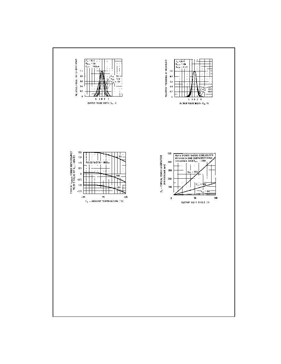
Typical Performance Characteristics
0% Point pulse width:
At V
CC
=
5V,
T
W
=
10.6
µ
s
At V
CC
=
10V,T
W
=
10
µ
s
At V
CC
=
15V,T
W
=
9.8
µ
s
Percentage of units within
+
4%:
At V
CC
=
5V,90% of units
At V
CC
=
10V,95% of units
At V
CC
=
15V,98% of units
FIGURE 1. Typical Distribution of Units for Output
Pulse Width
FIGURE 2. Typical Variation in Output Pulse Width vs
Temperature
0% Point pulse width:
At V
CC
=
5V,
T
W
=
1020
µ
s
At V
CC
=
10V,T
W
=
1000
µ
s
At V
CC
=
15V,T
W
=
982
µ
s
Percentage of units within
+
4%:
At V
CC
=
5V,95% of units
At V
CC
=
10V,97% of units
At V
CC
=
15V,98% of units
FIGURE 3. Typical Distribution of Units for Output
Pulse Width
FIGURE 4. Typical Power Dissipation per Package

5
www.fairchildsemi.com
MM74C221
Typical Performance Characteristics
(Continued)
Switching Time Waveforms
t
r
=
t
f
=
20 ns