© 2005 Fairchild Semiconductor Corporation
DS500165
www.fairchildsemi.com
July 1999
Revised February 2005
7
4
VC
X08
Low V
o
l
t
age Quad
2-
Inp
u
t AN
D Gate wit
h
3.
6V T
o
l
e
ra
nt Input
s
and Output
s
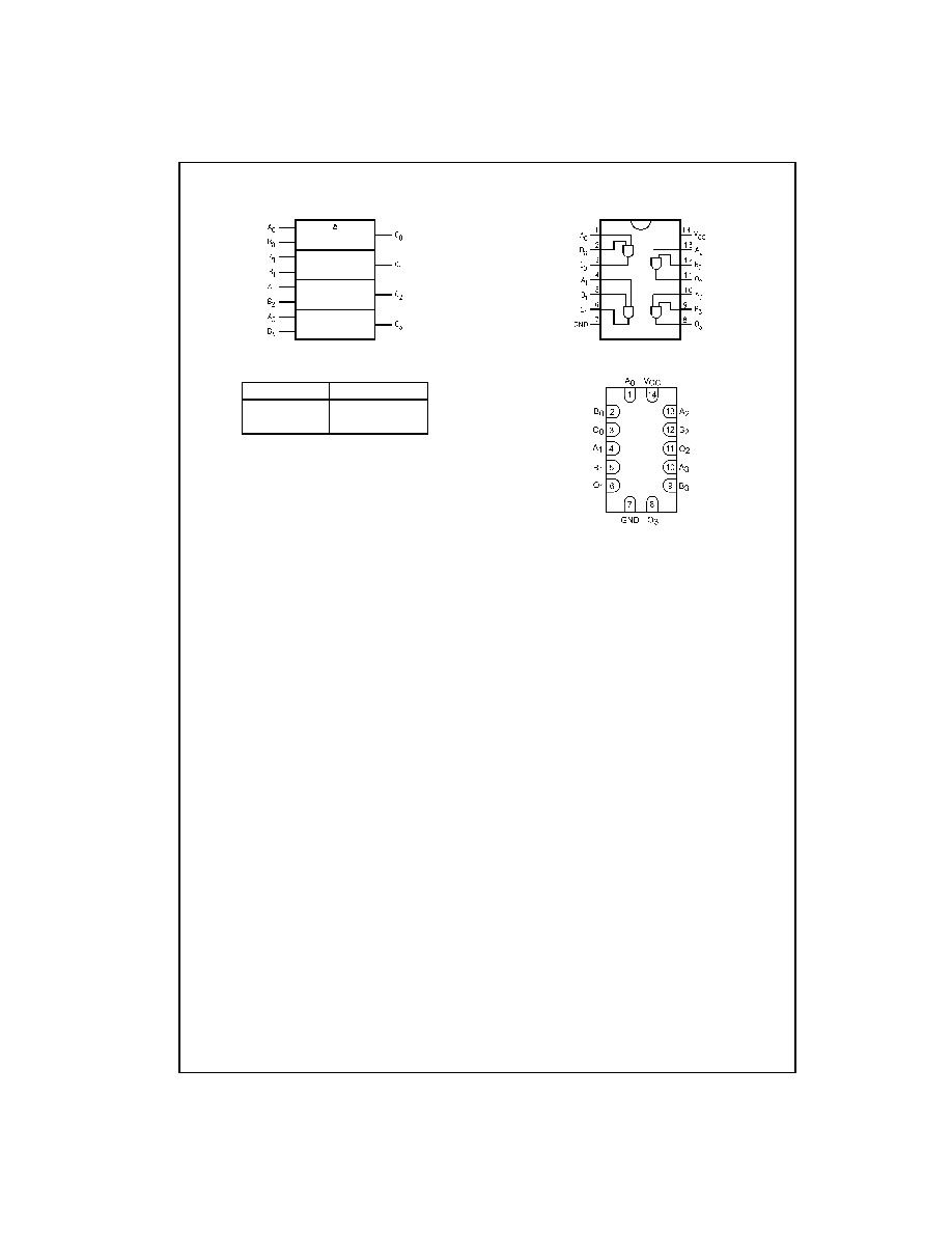
74VCX08
Low Voltage Quad 2-Input AND Gate with
3.6V Tolerant Inputs and Outputs
General Description
The VCX08 contains four 2-input AND gates. This product
is designed for low voltage (1.2V to 3.6V) V
CC
applications
with I/O compatibility up to 3.6V
The VCX08 is fabricated with an advanced CMOS technol-
ogy to achieve high-speed operation while maintaining low
CMOS power dissipation.
Features
s
1.2V to 3.6V V
CC
supply operation
s
3.6V tolerant inputs and outputs
s
t
PD
2.8 ns max for 3.0V to 3.6V V
CC
s
Power-off high impedance inputs and outputs
s
Static Drive (I
OH
/I
OL
)
r
24 mA @ 3.0V V
CC
s
Uses patented Quiet Series
•
noise/EMI reduction
circuitry
s
Latchup performance exceeds 300 mA
s
ESD performance:
Human body model
!
2000V
Machine model
!
250V
s
Leadless Pb-Free DQFN package
Ordering Code:
Pb-Free package per JEDEC J-STD-020B.
Note 1: Devices also available in Tape and Reel. Specify by appending the suffix letter "X" to the ordering code.
Note 2: DQFN package available in Tape and Reel only.
Note 3: "_NL" indicates Pb-Free package (per JEDEC J-STD-020B). Device available in Tape and Reel only.
Quiet Series
•
is a trademark of Fairchild Semiconductor Corporation.
Order Number
Package
Package Description
Number
74VCX08M
(Note 1)
M14A
14-Lead Small Outline Integrated Circuit (SOIC), JEDEC MS-012, 0.150" Narrow
74VCX08BQX
(Note 2)
MLP014A Pb-Free 14-Terminal Depopulated Quad Very-Thin Flat Pack No Leads (DQFN), JEDEC
MO-241, 2.5 x 3.0mm
74VCX08MTC
(Note 1)
MTC14
14-Lead Thin Shrink Small Outline Package (TSSOP), JEDEC MO-153, 4.4mm Wide
74VCX08MTCX_NL
(Note 3)
MTC14
Pb-Free 14-Lead Thin Shrink Small Outline Package (TSSOP), JEDEC MO-153, 4.4mm
Wide
3
www.fairchildsemi.com
7
4
VC
X08
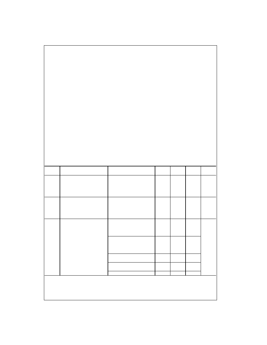
Absolute Maximum Ratings
(Note 4)
Recommended Operating
Conditions
(Note 6)
Note 4: The Absolute Maximum Ratings are those values beyond which
the safety of the device cannot be guaranteed. The device should not be
operated at these limits. The parametric values defined in the Electrical
Characteristics tables are not guaranteed at the Absolute Maximum Rat-
ings. The "Recommended Operating Conditions" table will define the condi-
tions for actual device operation.
Note 5: I
O
Absolute Maximum Rating must be observed.
Note 6: Floating or unused inputs must be held HIGH or LOW
DC Electrical Characteristics
Supply Voltage (V
CC
)
0.5V to
4.6V
DC Input Voltage (V
I
)
0.5V to
4.6V
Output Voltage (V
O
)
HIGH or LOW State (Note 5)
0.5V to V
CC
0.5V
V
CC
0V
0.5V to
4.6V
DC Input Diode Current (I
IK
)
V
I
0V
50 mA
DC Output Diode Current (I
OK
)
V
O
0V
50 mA
V
O
!
V
CC
50 mA
DC Output Source/Sink Current (I
OH
/I
OL
)
50 mA
DC V
CC
or Ground Current per
r
100 mA
Supply Pin (I
CC
or Ground)
Storage Temperature Range (T
stg
)
65
q
C to
150
q
C
Power Supply
Operating
1.2V to 3.6V
Input Voltage
0.3V to 3.6V
Output Voltage (V
O
)
HIGH or LOW State
0V to V
CC
Output Current in I
OH
/I
OL
V
CC
3.0V to 3.6V
r
24 mA
V
CC
2.3V to 2.7V
r
18 mA
V
CC
1.65V to 2.3V
r
6 mA
V
CC
1.4V to 1.6V
r
2 mA
V
CC
1.2V
r
100
P
A
Free Air Operating Temperature (T
A
)
40
q
C to
85
q
C
Minimum Input Edge Rate (
'
t/
'
V)
V
in
0.8V to 2.0V, V
CC
3.0V
10 ns/V
Symbol
Parameter
Conditions
V
CC
Min
Max
Units
(V)
V
IH
HIGH Level Input Voltage
2.7 to 3.6
2.0
V
2.3 to 2.7
1.6
1.65 to 2.3
0.65 x V
CC
1.4 to 1.6
0.65 x V
CC
1.2
0.65 x V
CC
V
IL
LOW Level Input Voltage
2.7 to 3.6
0.8
V
2.3 to 2.7
0.7
1.65 to 2.3
0.35 x V
CC
1.4 to 1.6
0.35 x V
CC
1.2
0.05 x V
CC
V
OH
HIGH Level Output Voltage
I
OH
100
P
A
2.7 to 3.6
V
CC
- 0.2
V
I
OH
12 mA
2.7
2.2
I
OH
18 mA
3.0
2.4
I
OH
24 mA
3.0
2.2
I
OH
100
P
A
2.3 to 2.7
V
CC
- 0.2
I
OH
6 mA
2.3
2.0
I
OH
12 mA
2.3
1.8
I
OH
18 mA
2.3
1.7
I
OH
100
P
A
1.65 to 2.3
V
CC
- 0.2
I
OH
6 mA
1.65
1.25
I
OH
100
P
A
1.4 to 1.6
V
CC
- 0.2
I
OH
2 mA
1.4
1.05
I
OH
100
P
A
1.2
V
CC
- 0.2
www.fairchildsemi.com
4
7
4
VC
X08
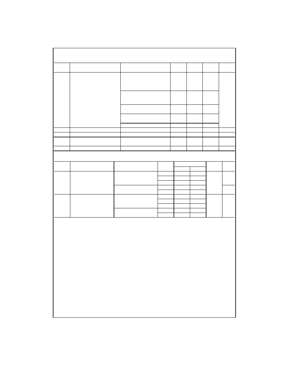
DC Electrical Characteristics
(Continued)
AC Electrical Characteristics
(Note 7)
Note 7: For C
L
pF, add approximately 300 ps to the AC maximum specification.
Note 8: Skew is defined as the absolute value of the difference between the actual propagation delay for any two separate outputs of the same device. The
specification applies to any outputs switching in the same direction, either HIGH-to-LOW (t
OSHL
) or LOW-to-HIGH (t
OSLH
).
Symbol
Parameter
Conditions
V
CC
Min
Max
Units
(V)
V
OL
LOW Level Output Voltage
I
OL
100
P
A
2.7 to 3.6
0.2
V
I
OL
12 mA
2.7
0.4
I
OL
18 mA
3.0
0.4
I
OL
24 mA
3.0
0.55
I
OL
100
P
A
2.3 to 2.7
0.2
I
OL
12 mA
2.3
0.4
I
OL
18 mA
2.3
0.6
I
OL
100
P
A
1.65 to 2.3
0.2
I
OL
6 mA
1.65
0.2
I
OL
100
P
A
1.4 to 1.6
0.2
I
OL
2 mA
1.4
0.35
I
OL
100
P
A
1.2
0.05
I
I
Input Leakage Current
0
d
V
I
d
3.6V
1.2 to 3.6
r
5.0
P
A
I
OFF
Power Off Leakage Current
0
d
(V
I
, V
O
)
d
3.6V
0
10
P
A
I
CC
Quiescent Supply Current
V
I
V
CC
or GND
1.2 to 3.6
20
P
A
V
CC
d
V
I
d
3.6V
1.2 to 3.6
r
20
'
I
CC
Increase in I
CC
per Input
V
IH
V
CC
0.6V
2.7 to 3.6
750
P
A
Symbol
Parameter
Conditions
V
CC
T
A
40
q
C to
85
q
C
Units
Figure
(V)
Min
Max
Number
t
PHL
Propagation Delay
C
L
30 pF, R
L
500
:
3.3
r
0.3
0.6
2.8
ns
Figures
1, 2
t
PLH
2.5
r
0.2
0.8
3.7
1.8
r
0.15
1.0
7.4
C
L
15 pF, R
L
2k
:
1.5
r
0.1
1.0
14.8
Figures
3, 4
1.2
1.5
37.0
t
OSHL
Output to Output Skew
C
L
30 pF, R
L
500
:
3.3
r
0.3
0.5
ns
t
OSLH
(Note 8)
2.5
r
0.2
0.5
1.8
r
0.15
0.75
C
L
15 pF, R
L
2k
:
1.5
r
0.1
1.5
1.2
1.5

5
www.fairchildsemi.com
7
4
VC
X08
Dynamic Switching Characteristics
Capacitance
AC Loading and Waveforms (V
CC
3.3V
r
0.3V to 1.8V
r
0.15V)
FIGURE 1. AC Test Circuit
FIGURE 2. Waveform for Inverting and Non-inverting Functions
Symbol
Parameter
Conditions
V
CC
T
A
25
q
C
Units
(V)
Typical
V
OLP
Quiet Output Dynamic Peak V
OL
C
L
30 pF, V
IH
V
CC
, V
IL
0V
1.8
0.25
V
2.5
0.6
3.3
0.8
V
OLV
Quiet Output Dynamic Valley V
OL
C
L
30 pF, V
IH
V
CC
, V
IL
0V
1.8
0.25
V
2.5
0.6
3.3
0.8
V
OHV
Quiet Output Dynamic Valley V
OH
C
L
30 pF, V
IH
V
CC
, V
IL
0V
1.8
1.5
V
2.5
1.9
3.3
2.2
Symbol
Parameter
Conditions
T
A
25
q
C
Units
Typical
C
IN
Input Capacitance
V
I
0V or V
CC
, V
CC
1.8V, 2.5V or 3.3V
6.0
pF
C
OUT
Output Capacitance
V
I
0V or V
CC
, V
CC
1.8V, 2.5V or 3.3V
7.0
pF
C
PD
Power Dissipation Capacitance
V
I
0V or V
CC
, f
10 MHz, V
CC
1.8V, 2.5V or 3.3V
20.0
pF
TEST
SWITCH
t
PLH
, t
PHL
Open
Symbol
V
CC
3.3V
r
0.3V
2.5V
r
0.2V
1.8V
r
0.15V
V
mi
1.5V
V
CC
/2
V
CC
/2
V
mo
1.5V
V
CC
/2
V
CC
/2