© 1999 Fairchild Semiconductor Corporation
ds500164
www.fairchildsemi.com
July 1999
Revised July 1999
7
4
VC
X13
2
Low V
o
l
t
a
ge
Quad 2-I
nput
NAND
Gat
e
wi
th Schm
i
t
t
T
r
i
gger Input
s and
3.
6V T
o
ler
ant Input
s and
Out
-
pu
ts
74VCX132
Low Voltage Quad 2-Input NAND Gate with
Schmitt Trigger Inputs and 3.6V Tolerant Inputs
and Outputs
General Description
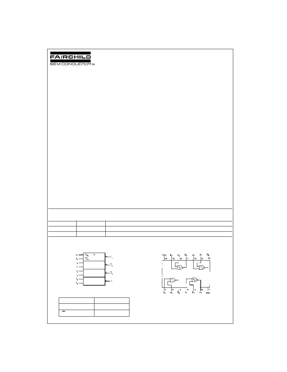
The VCX132 contains four 2-input NAND gates with
Schmitt Trigger Inputs. The pin configuration and function
are the same as the VCX00 except the inputs have hyster-
esis between the positive-going and negative-going input
thresholds. This hysteresis is useful for transforming slowly
switching input signals into sharply defined, jitter-free out-
put signals. This product should be used where noise mar-
gin greater than that of conventional gates is required.
The VCX132 is designed for low voltage (1.65V to 3.6V)
V
CC
applications with I/O compatibility up to 3.6V.
This product is fabricated with an advanced CMOS tech-
nology to achieve high-speed operation while maintaining
low CMOS power dissipation.
Features
s
1.65V-3.6V V
CC
supply operation
s
3.6V tolerant inputs and outputs
s
t
PD
3.3 ns max for 3.0V to 3.6V V
CC
4.1 ns max for 2.3V to 2.7V V
CC
8.2 ns max for 1.65V to 1.95V V
CC
s
Power-off high impedance inputs and outputs
s
Static Drive (I
OH
/I
OL
)
±
24 mA @ 3.0V V
CC
±
18 mA @ 2.3V V
CC
±
6
mA @
1.65V
V
CC
s
Uses patented Quiet Series
TM
noise/EMI reduction
circuitry
s
Latchup performance exceeds 300 mA
s
ESD performance:
Human body model
>
2000V
Machine model
>
250V
Ordering Code:
Devices also available in Tape and Reel. Specify by appending suffix letter "X" to the ordering code.
Logic Diagram
Pin Descriptions
Connection Diagram
Quiet Series
TM
is a trademark of Fairchild Semiconductor Corporation.
Order Number
Package Number
Package Description
74VCX132M
M14A
14-Lead Small Outline Integrated Circuit (SOIC), JEDEC MS-120, 0.150" Narrow
74VCX132MTC
MTC14
14-Lead Thin Shrink Small Outline Package (TSSOP), JEDEC MO-153, 4.4mm Wide
Pin Name
Description
A
n
, B
n
Inputs
O
n
Outputs
www.fairchildsemi.com
2
74
V
CX132
Absolute Maximum Ratings
(Note 1)
Recommended Operating
Conditions
(Note 3)
Note 1: The "Absolute Maximum Ratings" are those values beyond which
the safety of the device cannot be guaranteed. The device should not be
operated at these limits. The parametric values defined in the Electrical
Characteristics tables are not guaranteed at the absolute maximum ratings.
The "Recommended Operating Conditions" table will define the conditions
for actual device operation.
Note 2: I
O
Absolute Maximum Rating must be observed.
Note 3: Floating or unused inputs must be held HIGH or LOW.
DC Electrical Characteristics (2.7V
<
V
CC
3.6V)
Supply Voltage (V
CC
)
-
0.5V to
+
4.6V
DC Input Voltage (V
I
)
-
0.5V to 4.6V
DC Output Voltage (V
O
)
HIGH or LOW State (Note 2)
-
0.5V to V
CC
+
0.5V
V
CC
=
0V
-
0.5V to
+
4.6V
DC Input Diode Current (I
IK
)
V
I
<
0V
-
50 mA
DC Output Diode Current (I
OK
)
V
O
<
0V
-
50 mA
V
O
>
V
CC
+
50 mA
DC Output Source/Sink Current
±
50 mA
(I
OH
/I
OL
)
DC V
CC
or Ground Current per
±
100 mA
Supply Pin (I
CC
or Ground)
Storage Temperature (T
STG
)
-
65
∞
C to
+
150
∞
C
Power Supply
Operating
1.65V to 3.6V
Data Retention Only
1.2V to 3.6V
Input Voltage
-
0.3V to 3.6V
Output Voltage (V
O
)
HIGH or LOW State
0V to V
CC
Output Current in I
OH
/I
OL
V
CC
=
3.0V to 3.6V
±
24 mA
V
CC
=
2.3V to 2.7V
±
18 mA
V
CC
=
1.65V to 2.3V
±
6 mA
Free Air Operating Temperature (T
A
)
-
40
∞
C to
+
85
∞
C
Symbol
Parameter
Conditions
V
CC
(V)
Min
Max
Units
V
t
+
Positive Threshold
3.6
2.2
V
3.0
2.0
V
t
-
Negative Threshold
3.6
0.8
V
3.0
0.7
V
H
Input Hysteresis
3.6
0.3
1.2
V
3.0
0.3
1.2
V
OH
HIGH Level Output Voltage
I
OH
=
-
100
µ
A
2.7≠3.6
V
CC
≠0.2
V
I
OH
=
-
12 mA
2.7
2.2
I
OH
=
-
18 mA
3.0
2.4
I
OH
=
-
24mA
3.0
2.2
V
OL
LOW Level Output Voltage
I
OL
=
100
µ
A
2.7≠3.6
0.2
V
I
OL
=
12
µ
A
2.7
0.4
I
OL
=
18 mA
3.0
0.4
I
OL
=
24 mA
3.0
0.55
I
I
Input Leakage Current
0
V
I
3.6V
2.7≠3.6
±
15.0
µ
A
I
OFF
Power Off Leakage Current
0
(V
I
, V
O
)
3.6V
0
10
µ
A
I
CC
Quiescent Supply Current
V
I
=
V
CC
or GND
2.7≠3.6
20
µ
A
V
CC
V
I
3.6V
2.7≠3.6
±
20
I
CC
Increase in I
CC
per Input
V
IH
=
V
CC
≠ 0.6V
2.7≠3.6
750
µ
A
3
www.fairchildsemi.com
7
4
VC
X13
2
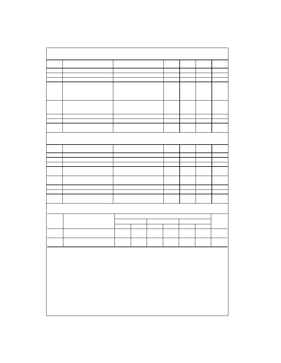
DC Electrical Characteristics (2.3V
V
CC
2.7V)
DC Electrical Characteristics (1.65V
V
CC
<
2.3V)
AC Electrical Characteristics
(Note 4)
Note 4: For C
L
=
50 pF, add approximately 300 ps to the AC maximum specification.
Note 5: Skew is defined as the absolute value of the difference between the actual propagation delay for any two separate outputs of the same device. The
specification applies to any outputs switching in the same direction, either HIGH-to-LOW (t
OSHL
) or LOW
-
to
-
HIGH (t
OSLH
).
Symbol
Parameter
Conditions
V
CC
(V)
Min
Max
Units
V
t
+
Positive Threshold
2.3
1.6
V
V
t
-
Negative Threshold
2.3
0.5
V
V
T
Input Hysteresis
2.3
0.3
1.0
V
V
OH
HIGH Level Output Voltage
I
OH
=
-
100
µ
A
2.3≠2.7
V
CC
≠0.2
V
I
OH
=
-
6 mA
2.3
2.0
I
OH
=
-
12 mA
2.3
1.8
I
OH
=
-
18 mA
2.3
1.7
V
OL
LOW Level Output Voltage
I
OL
=
100
µ
A
2.3≠2.7
0.2
V
I
OL
=
12
µ
A
2.3
0.4
I
OL
=
18 mA
2.3
0.6
I
I
Input Leakage Current
0
V
I
3.6V
2.3≠2.7
±
5.0
µ
A
I
OFF
Power Off Leakage Current
0
(V
I
, V
O
)
3.6V
0
10
µ
A
I
CC
Quiescent Supply Current
V
I
=
V
CC
or GND
2.3≠2.7
20
µ
A
V
CC
V
I
3.6V
2.3≠2.7
±
20
Symbol
Parameter
Conditions
V
CC
(V)
Min
Max
Units
V
t
+
Positive Threshold
1.65
1.3
V
V
t
-
Negative Threshold
1.65
0.25
V
V
T
Input Hysteresis
1.65
0.2
0.9
V
V
OH
HIGH Level Output Voltage
I
OH
=
-
100
µ
A
1.65≠2.3
V
CC
≠0.2
V
I
OH
=
-
6 mA
1.65
1.25
V
OL
LOW Level Output Voltage
I
OL
=
100
µ
A
1.65≠2.3
0.2
V
I
OL
=
6 mA
1.65
0.3
I
I
Input Leakage Current
0
V
I
3.6V
1.65≠2.3
±
5.0
µ
A
I
OFF
Power Off Leakage Current
0
(V
I
, V
O
)
3.6V
0
10
µ
A
I
CC
Quiescent Supply Current
V
I
=
V
CC
or GND
1.65≠2.3
20
µ
A
V
CC
V
I
3.6V
1.65≠2.3
±
20
T
A
=
-
40
∞
C to
+
85
∞
C, C
L
=
30 pF, R
L
=
500
Symbol
Parameter
V
CC
=
3.3 V
±
0.3V
V
CC
=
2.5 V
±
0.2V
V
CC
=
1.8 V
±
0.15V
Units
Min
Max
Min
Max
Min
Max
t
PHL
Propagation Delay
0.6
3.3
0.8
4.1
1.0
8.2
ns
t
PLH
t
OSHL
Output to Output
0.5
0.5
0.75
ns
t
OSLH
Skew (Note 5)
www.fairchildsemi.com
4
74
V
CX132
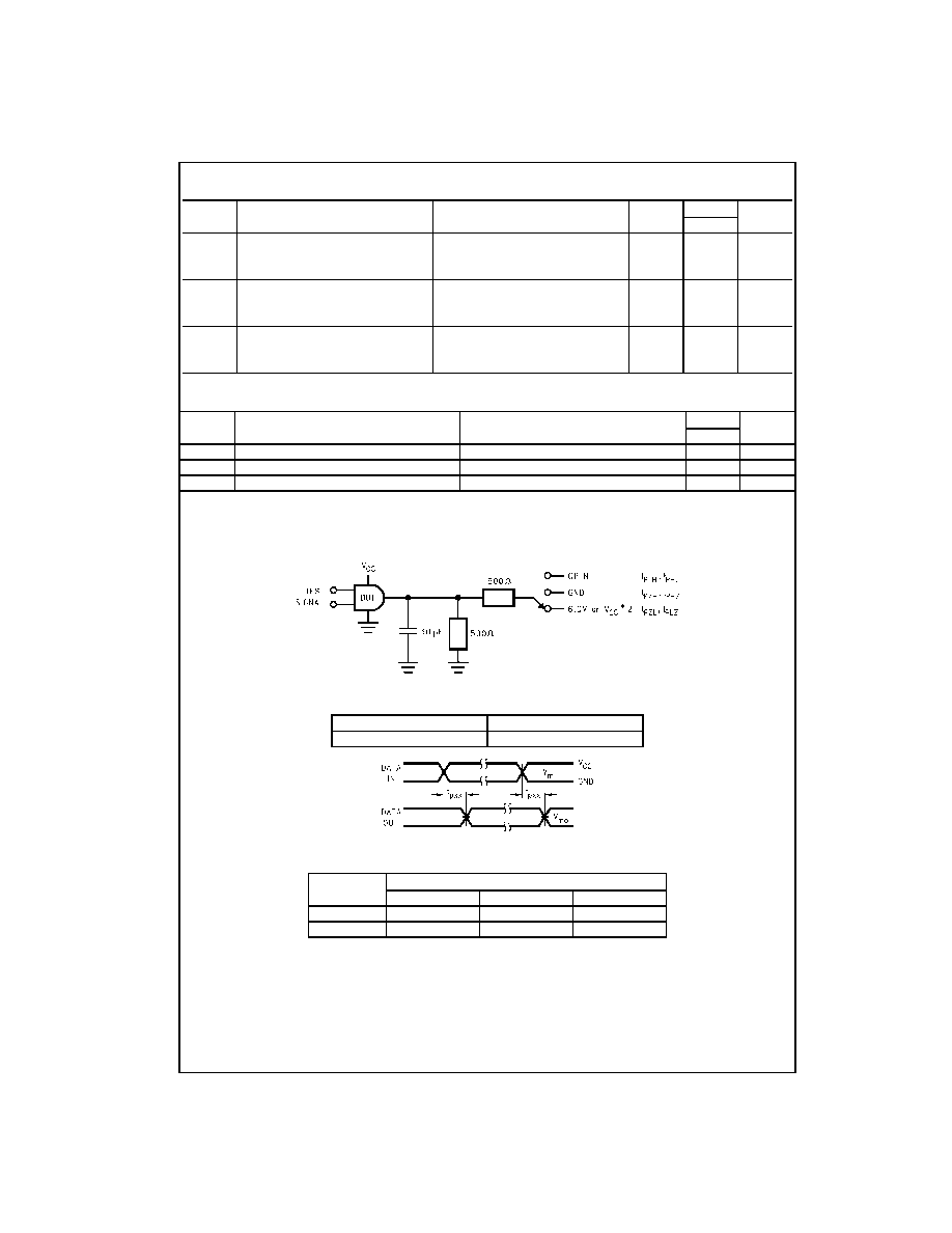
Dynamic Switching Characteristics
Capacitance
AC Loading and Waveforms
FIGURE 1. AC Test Circuit
FIGURE 2. Waveform for Inverting and Non-inverting Functions
Symbol
Parameter
Conditions
V
CC
(V)
T
A
=
+
25
∞
C
Units
Typical
V
OLP
Quiet Output Dynamic
C
L
=
30 pF, V
IH
=
V
CC
, V
IL
=
0V
1.8
0.25
V
Peak V
OL
2.5
0.6
3.3
0.8
V
OLV
Quiet Output Dynamic
C
L
=
30 pF, V
IH
=
V
CC
, V
IL
=
0V
1.8
-
0.25
V
Valley V
OL
2.5
-
0.6
3.3
-
0.8
V
OHV
Quiet Output Dynamic
C
L
=
30 pF, V
IH
=
V
CC
, V
IL
=
0V
1.8
1.5
V
Valley V
OH
2.5
1.9
3.3
2.2
Symbol
Parameter
Conditions
T
A
=
+
25
∞
C
Units
Typical
C
IN
Input Capacitance
V
I
=
0V or V
CC
, V
CC
=
1.8V, 2.5V or 3.3V
6
pF
C
OUT
Output Capacitance
V
I
=
0V or V
CC
, V
CC
=
1.8V, 2.5V or 3.3V
7
pF
C
PD
Power Dissipation Capacitance
V
I
=
0V or V
CC
, f
=
10MHz, V
CC
=
1.8V, 2.5V or 3.3V
20
pF
TEST
SWITCH
t
PLH
, t
PHL
Open
Symbol
V
CC
3.3V
±
0.3V
2.5V
±
0.2V
1.8V
±
0.15V
V
mi
1.5V
V
CC
/2
V
CC
/2
V
mo
1.5V
V
CC
/2
V
CC
/2
5
www.fairchildsemi.com
7
4
VC
X13
2
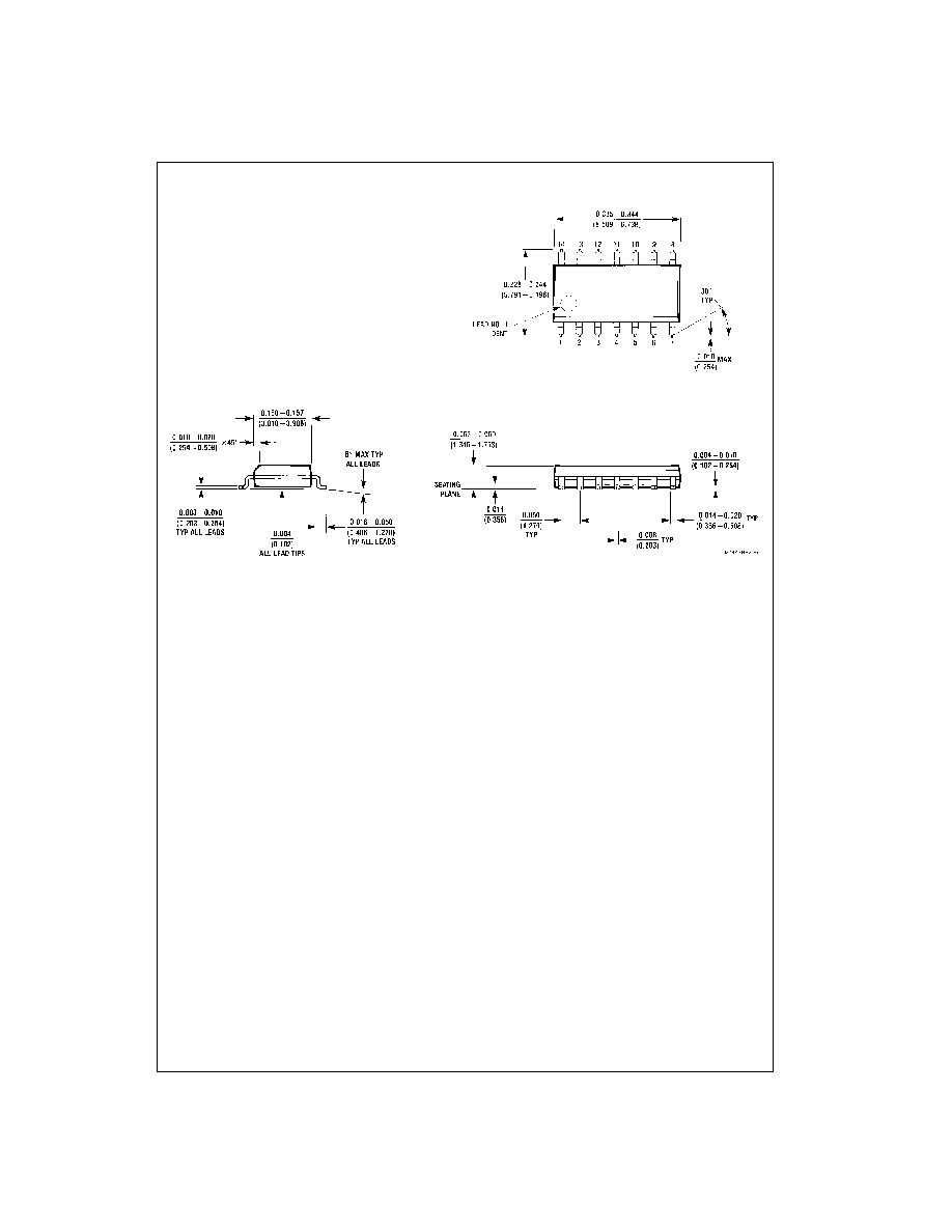
Physical Dimensions
inches (millimeters) unless otherwise noted
14-Lead Small Outline Integrated Circuit (SOIC), JEDEC MS-120, 0.150" Narrow
Package Number M14A