October 1996
Revised April 1999
7
4
VC
X16
2245 Low V
o
l
t
age 16-Bi
t Bi
dir
ecti
onal
T
r
ansc
eiver
wit
h
3.6V T
o
l
e
rant
Input
s and Outp
uts and 26
Ser
i
es
Res
i
st
ors in A
Por
t
Output
s
� 1999 Fairchild Semiconductor Corporation
DS500048.prf
www.fairchildsemi.com
74VCX162245
Low Voltage 16-Bit Bidirectional Transceiver with 3.6V
Tolerant Inputs and Outputs and 26
Series Resistors in
A Port Outputs
General Description
The VCX162245 contains sixteen non-inverting bidirec-
tional buffers with 3-STATE outputs and is intended for bus
oriented applications. The device is byte controlled. Each
byte has separate 3-STATE control inputs which can be
shorted together for full 16-bit operation. The T/R inputs
determine the direction of data flow through the device.
The OE inputs disable both the A and B ports by placing
them in a high impedance state.
The 74VCX162245 is designed for low voltage (1.65V to
3.6V) V
CC
applications with I/O compatibility up to 3.6V.
The 74VCX162245 is also designed with 26
series resis-
tance in the A Port outputs. This design reduces line noise
in applications such as memory address drivers, clock driv-
ers, and bus transceivers/transmitters.
The 74VCX162245 is fabricated with an advanced CMOS
technology to achieve high speed operation while maintain-
ing low CMOS power dissipation.
Features
s
1.65V�3.6V V
CC
supply operation
s
3.6V tolerant inputs and outputs
s
26
series resistors in A port outputs
s
t
PD
(B to A)
3.4 ns max for 3.0V to 3.6V V
CC
4.3 ns max for 2.3V to 2.7V V
CC
8.6 ns max for 1.65V to 1.95V V
CC
s
Power-down high impedance inputs and outputs
s
Supports live insertion/withdrawal (Note 1)
s
Static Drive (I
OH
/I
OL
A outputs)
�
12 mA @ 3.0V V
CC
�
8 mA @ 2.3V V
CC
�
3
mA @
1.65V
V
CC
s
Uses patented noise/EMI reduction circuitry
s
Latchup performance exceeds 300 mA
s
ESD performance:
Human body model
>
2000V
Machine model
>
200V
Note 1: To ensure the high-impedance state during power up or power
down, OE should be tied to V
CC
through a pull-up resistor; the minimum
value of the resistor is determined by the current-sourcing capability of the
driver.
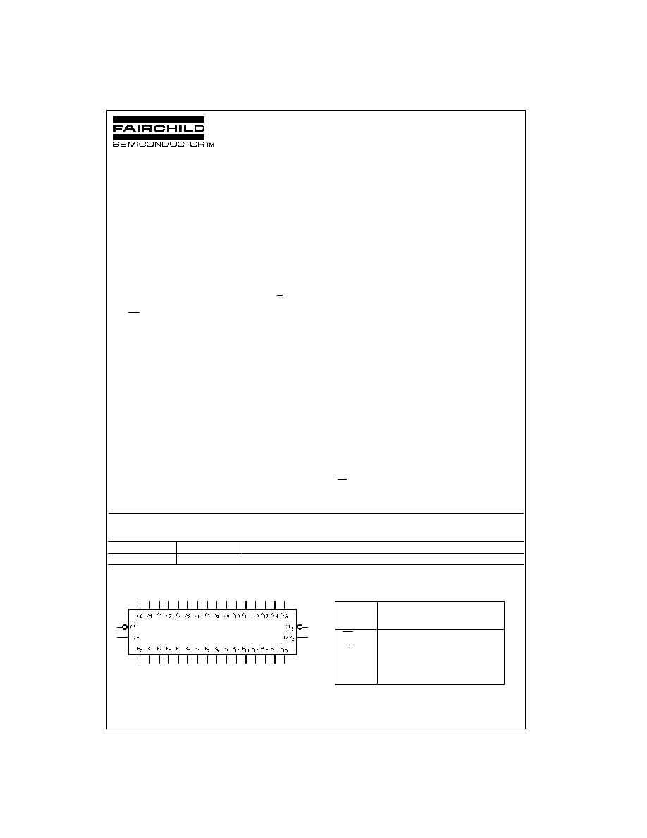
Ordering Code:
Devices also available in Tape and Reel. Specify by appending the suffix letter "X" to the ordering code.
Logic Symbol
Pin Descriptions
Order Number
Package Number
Package Description
74VCX162245MTD
MTD48
48-Lead Thin Shrink Small Outline Package (TSSOP), JEDEC MO-153, 6.1mm Wide
Pin
Description
Names
OE
n
Output Enable Input
T/R
n
Transmit/Receive Input
A
0
�A
15
Side A Inputs or 3-STATE Outputs
B
0
�B
15
Side B Inputs or 3-STATE Outputs
www.fairchildsemi.com
2
74VCX162245
Connection Diagram
Truth Tables
H
=
HIGH Voltage Level
L
=
LOW Voltage Level
X
=
Immaterial (HIGH or LOW, inputs and I/O's may not float)
Z
=
High Impedance
Logic Diagram
Inputs
Outputs
OE
1
T/R
1
L
L
Bus B
0
�B
7
Data to Bus A
0
�A
7
L
H
Bus A
0
�A
7
Data to Bus B
0
�B
7
H
X
HIGH Z State on A
0
�A
7
, B
0
�B
7
Inputs
Outputs
OE
2
T/R
2
L
L
Bus B
8
�B
15
Data to Bus A
8
�A
15
L
H
Bus A
8
�A
15
Data to Bus B
8
�B
15
H
X
HIGH Z State on A
8
�A
15
, B
8
�B
15
3
www.fairchildsemi.com
7
4
VC
X16
2245
Absolute Maximum Ratings
(Note 2)
Recommended Operating
Conditions
(Note 4)
Note 2: The "Absolute Maximum Ratings" are those values beyond which
the safety of the device cannot be guaranteed. The device should not be
operated at these limits. The parametric values defined in the Electrical
Characteristics tables are not guaranteed at the Absolute Maximum Rat-
ings. The Recommended Operating Conditions tables will define the condi-
tions for actual device operation.
Note 3: I
O
Absolute Maximum Rating must be observed.
Note 4: Floating or unused pins (inputs or I/O's) must be held HIGH or
LOW.
DC Electrical Characteristics (2.7V
<
V
CC
3.6V)
Note 5: Outputs disabled or 3-STATE only.
Supply Voltage (V
CC
)
-
0.5V to
+
4.6V
DC Input Voltage (V
I
)
-
0.5V to
+
4.6V
Output Voltage (V
O
)
Outputs 3-State
-
0.5V to
+
4.6V
Outputs Active (Note 3)
-
0.5 to V
CC
+
0.5V
DC Input Diode Current (I
IK
) V
I
<
0V
-
50 mA
DC Output Diode Current (I
OK
)
V
O
<
0V
-
50 mA
V
O
>
V
CC
+
50 mA
DC Output Source/Sink Current
(I
OH
/I
OL
)
�
50 mA
DC V
CC
or Ground Current per
Supply Pin (I
CC
or Ground)
�
100 mA
Storage Temperature Range (T
STG
)
-
65
�
C to
+
150
�
C
Power Supply
Operating
1.65V to 3.6V
Data Retention Only
1.2V to 3.6V
Input Voltage
-
0.3V to 3.6V
Output Voltage (V
O
)
Output in Active States
0V to V
CC
Output in 3-STATE
0.0V to 3.6V
Output Current in I
OH
/I
OL
-A Outputs
V
CC
=
3.0V to 3.6V
�
12 mA
V
CC
=
2.3V to 2.7V
�
8 mA
V
CC
=
1.65V to 1.95V
�
3 mA
Output Current in
�
I
OH
/I
OL
-B Outputs
V
CC
=
3.0V to 3.6V
�
24mA
V
CC
=
2.3V to 2.7V
�
18mA
V
CC
=
1.65V to 2.3V
�
6mA
Free Air Operating Temperature (T
A
)
-
40
�
C to
+
85
�
C
Minimum Input Edge Rate (
t/
V)
V
IN
=
0.8V to 2.0V, V
CC
=
3.0V
10 ns/V
Symbol
Parameter
Conditions
V
CC
Min
Max
Units
(V)
V
IH
HIGH Level Input Voltage
2.7�3.6
2.0
V
V
IL
LOW Level Input Voltage
2.7�3.6
0.8
V
V
OH
HIGH Level Output Voltage
I
OH
=
-
100
�
A
2.7�3.6
V
CC
-
0.2
A Outputs
I
OH
=
-
6 mA
2.7
2.2
V
I
OH
=
-
8 mA
3.0
2.4
I
OH
=
-
12 mA
3.0
2.2
HIGH Level Output Voltage
I
OH
=
-
100
�
A
2.7�3.6
V
CC
-
0.2
B Outputs
I
OH
=
-
12 mA
2.7
2.2
V
I
OH
=
-
18 mA
3.0
2.4
I
OH
=
-
24 mA
3.0
2.2
V
OL
LOW Level Output Voltage
I
OL
=
100
�
A
2.7�3.6
0.2
A Outputs
I
OL
=
6 mA
2.7
0.4
V
I
OL
=
8 mA
3.0
0.55
I
OL
=
12 mA
3.0
0.8
LOW Level Output Voltage
I
OL
=
100
�
A
2.7�3.6
0.2
B Outputs
I
OL
=
12 mA
2.7
0.4
V
I
OL
=
18 mA
3.0
0.4
I
OL
=
24 mA
3.0
0.55
I
I
Input Leakage Current
0V
V
I
3.6V
2.7�3.6
�
5.0
�
A
I
OZ
3-STATE Output Leakage
0V
V
O
3.6V
2.7�3.6
�
10
�
A
V
I
=
V
IH
or V
IL
I
OFF
Power Off Leakage Current
0V
(V
I
, V
O
)
3.6V
0
10
�
A
I
CC
Quiescent Supply Current
V
I
=
V
CC
or GND
2.7�3.6
20
�
A
V
CC
(V
I
, V
O
)
3.6V (Note 5)
2.7�3.6
�
20
I
CC
Increase in I
CC
per Input
V
IH
=
V
CC
-
0.6V
2.7�3.6
750
�
A
www.fairchildsemi.com
4
74VCX162245
DC Electrical Characteristics (2.3V
V
CC
2.7V)
Note 6: Outputs disabled or 3-STATE only.
DC Electrical Characteristics (1.65V
V
CC
<
2.3V)
Note 7: Outputs disabled or 3-STATE only.
Symbol
Parameter
Conditions
V
CC
Min
Max
Units
(V)
V
IH
HIGH Level Input Voltage
2.3�2.7
1.6
V
V
IL
LOW Level Input Voltage
2.3�2.7
0.7
V
V
OH
HIGH Level Output Voltage
I
OH
=
-
100
�
A
2.3�2.7
V
CC
-
0.2
V
A Outputs
I
OH
=
-
4 mA
2.3
2.0
I
OH
=
-
6 mA
2.3
1.8
I
OH
=
-
8 mA
2.3
1.7
HIGH Level Output Voltage
I
OH
=
-
100
�
A
2.3�2.7
V
CC
-
0.2
B Outputs
I
OH
=
-
6 mA
2.3
2.0
V
I
OH
=
-
12 mA
2.3
1.8
I
OH
=
-
18 mA
2.3
1.7
V
OL
LOW Level Output Voltage
I
OL
=
100
�
A
2.3�2.7
0.2
A Outputs
I
OL
=
6 mA
2.3
0.4
V
I
OL
=
8 mA
2.3
0.6
LOW Level Output Voltage
I
OL
=
100
�
A
2.3�2.7
0.2
B Outputs
I
OL
=
12 mA
2.3
0.4
V
I
OL
=
18 mA
2.3
0.6
I
I
Input Leakage Current
0
V
I
3.6V
2.3�2.7
�
5.0
�
A
I
OZ
3-STATE Output Leakage
0
V
O
3.6V
2.3�2.7
�
10
�
A
V
I
=
V
IH
or V
IL
I
OFF
Power Off Leakage Current
0
(V
I
, V
O
)
3.6V
0
10
�
A
I
CC
Quiescent Supply Current
V
I
=
V
CC
or GND
2.3�2.7
20
�
A
V
CC
(V
I
, V
O
)
3.6V (Note 6)
2.3�2.7
�
20
Symbol
Parameter
Conditions
V
CC
Min
Max
Units
(V)
V
IH
HIGH Level Input Voltage
1.65-2.3
0.65
�
V
CC
V
V
IL
LOW Level Input Voltage
1.65-2.3
0.35
�
V
CC
V
V
OH
HIGH Level Output Voltage
I
OH
=
-
100
�
A
1.65-2.3
V
CC
-
0.2
V
A Outputs
I
OH
=
-
3 mA
1.65
1.4
HIGH Level Output Voltage
I
OH
=
-
100
�
A
1.65-2.3
V
CC
-
0.2
V
B Outputs
I
OH
=
-
6 mA
1.65
1.25
V
OL
LOW Level Output Voltage
I
OL
=
100
�
A
1.65-2.3
0.2
V
A Outputs
I
OL
=
3 mA
1.65
0.3
LOW Level Output Voltage
I
OL
=
100
�
A
1.65-2.3
0.2
V
B Outputs
I
OL
=
6 mA
1.65
0.3
I
I
Input Leakage Current
0
V
I
3.6V
1.65-2.3
�
5.0
�
A
I
OZ
3-STATE Output Leakage
0
V
O
3.6V
1.65-2.3
�
10
�
A
V
I
=
V
IH
or V
IL
I
OFF
Power Off Leakage Current
0
(V
I
, V
O
)
3.6V
0
10
�
A
I
CC
Quiescent Supply Current
V
I
=
V
CC
or GND
1.65-2.3
20
�
A
V
CC
(V
I
, V
O
)
3.6V (Note 7)
1.65-2.3
�
20

5
www.fairchildsemi.com
7
4
VC
X16
2245
AC Electrical Characteristics
(Note 8)
Note 8: For C
L
=
50pF, add approximately 300ps to the AC maximum specification.
Note 9: Skew is defined as the absolute value of the difference between the actual propagation delay for any two separate outputs of the same device. The
specification applies to any outputs switching in the same direction, either HIGH-to-LOW (t
OSHL
) or LOW
-
to
-
HIGH (t
OSLH
).
Dynamic Switching Characteristics
Capacitance
T
A
=
-
40
�
C to
+
85
�
C, C
L
=
30 pF, R
L
=
500
Symbol
Parameter
V
CC
=
3.3V
�
0.3V
V
CC
=
2.5
�
0.2V
V
CC
=
1.8V
�
0.15
Units
Min
Max
Min
Max
Min
Max
t
PHL
, t
PLH
Prop Delay, A to B
0.8
2.5
1.0
3.0
1.5
6.0
ns
t
PHL
, t
PLH
Prop Delay, B to A
0.8
3.4
1.0
4.3
1.5
8.6
ns
t
PZL
, t
PZH
Output Enable Time, A to B
0.8
3.8
1.0
4.9
1.5
9.3
ns
t
PZL
, t
PZH
Output Enable Time, B to A
0.8
4.2
1.0
5.7
1.5
9.8
ns
t
PLZ
, t
PHZ
Output Disable Time, A to B
0.8
3.7
1.0
4.2
1.5
7.6
ns
t
PLZ
, t
PHZ
Output Disable Time, B to A
0.8
4.1
1.0
4.8
1.5
8.6
ns
t
OSHL
Output to Output
0.5
0.5
0.75
ns
t
OSLH
Skew (Note 9)
Symbol
Parameter
Conditions
V
CC
(V)
T
A
=
+
25
�
C
Units
Typical
V
OLP
Quiet Output Dynamic
Peak V
OL
, A to B
C
L
=
30 pF, V
IH
=
V
CC
, V
IL
=
0V
1.8
2.5
3.3
0.25
0.6
0.8
V
V
OLP
Quiet Output Dynamic
Peak V
OL
, B to A
C
L
=
30 pF, V
IH
=
V
CC
, V
IL
=
0V
1.8
2.5
3.3
0.15
0.25
0.35
V
V
OLV
Quiet Output Dynamic
Valley V
OL
, A to B
C
L
=
30 pF, V
IH
=
V
CC
, V
IL
=
0V
1.8
2.5
3.3
-
0.25
-
0.6
-
0.8
V
V
OLV
Quiet Output Dynamic
Valley V
OL
, B to A
C
L
=
30 pF, V
IH
=
V
CC
, V
IL
=
0V
1.8
2.5
3.3
0.15
-
0.25
-
0.35
V
V
OHV
Quiet Output Dynamic
Valley V
OH
, A to B
C
L
=
30 pF, V
IH
=
V
CC
, V
IL
=
0V
1.8
2.5
3.3
1.5
1.9
2.2
V
V
OHV
Quiet Output Dynamic
Valley V
OH
, B to A
C
L
=
30 pF, V
IH
=
V
CC
, V
IL
=
0V
1.8
2.5
3.3
1.55
2.05
2.65
V
Symbol
Parameter
Conditions
T
A
=
+
25
�
C
Units
C
IN
Input Capacitance
V
CC
=
1.8V, 2.5V, or 3.3V, V
I
=
0V or V
CC
6
pF
C
I/O
Output Capacitance
V
I
=
0V, or V
CC
, V
CC
=
1.8V, 2.5V or 3.3V
7
pF
C
PD
Power Dissipation Capacitance
V
I
=
0V or V
CC
, f
=
10 MHz
20
pF
V
CC
=
1.8V, 2.5V or 3.3V