© 2005 Fairchild Semiconductor Corporation
DS012168
www.fairchildsemi.com
October 1996
Revised June 2005
7
4
VC
X16
244 Lo
w
V
o
lt
age
16-
Bit
Buf
f
er
/Li
ne
D
r
ive
r
wi
th
3.
6V T
o
l
e
rant
I
nput
s
and Out
put
s
74VCX16244
Low Voltage 16-Bit Buffer/Line Driver with
3.6V Tolerant Inputs and Outputs
General Description
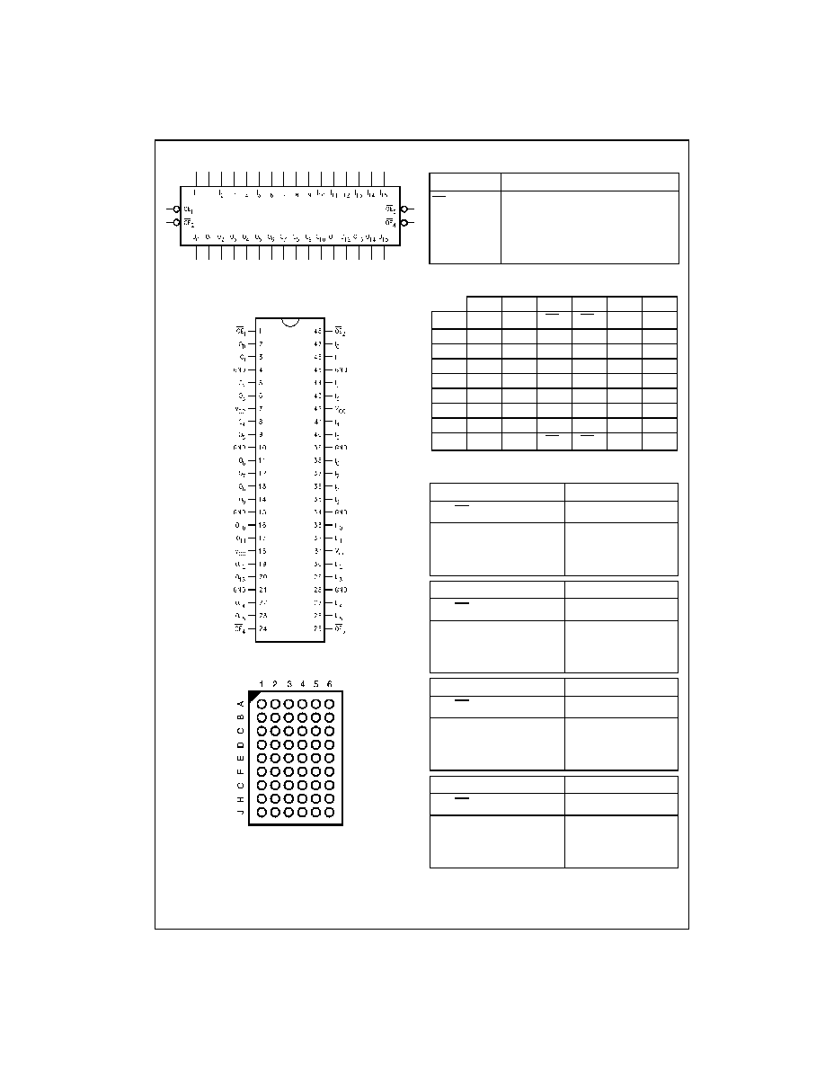
The VCX16244 contains sixteen non-inverting buffers with
3-STATE outputs to be employed as a memory and
address driver, clock driver, or bus oriented transmitter/
receiver. The device is nibble (4-bit) controlled. Each nibble
has separate 3-STATE control inputs which can be shorted
together for full 16-bit operation.
The 74VCX16244 is designed for low voltage (1.2V to
3.6V) V
CC
applications with I/O capability up to 3.6V.
The 74VCX16244 is fabricated with an advanced CMOS
technology to achieve high speed operation while maintain-
ing low CMOS power dissipation.
Features
s
1.2V to 3.6V V
CC
supply operation
s
3.6V tolerant inputs and outputs
s
t
PD
2.5 ns max for 3.0V to 3.6V V
CC
s
Power-off high impedance inputs and outputs
s
Supports live insertion and withdrawal (Note 1)
s
Static Drive (I
OH
/I
OL
)
r
24 mA @ 3.0V V
CC
s
Uses patented noise/EMI reduction circuitry
s
Latch-up performance exceeds 300 mA
s
ESD performance:
Human body model
!
2000V
Machine model
!
200V
s
Also packaged in plastic Fine-Pitch Ball Grid Array
(FBGA)
Note 1: To ensure the high-impedance state during power up or power
down, OE should be tied to V
CC
through a pull-up resistor; the minimum
value of the resistor is determined by the current-sourcing capability of the
driver.
Ordering Code:
Note 2: Ordering Code "G" indicates Tray.
Note 3: Devices also available in Tape and Reel. Specify by appending the suffix letter "X" to the ordering code.
Order Number
Package Number
Package Description
74VCX16244G
(Note 2)(Note 3)
BGA54A
54-Ball Fine-Pitch Ball Grid Array (FBGA), JEDEC MO-205, 5.5mm Wide
74VCX16244MTD
(Note 3)
MTD48
48-Lead Thin Shrink Small Outline Package (TSSOP), JEDEC MO-153, 6.1mm Wide
3
www.fairchildsemi.com
7
4
VC
X16
244
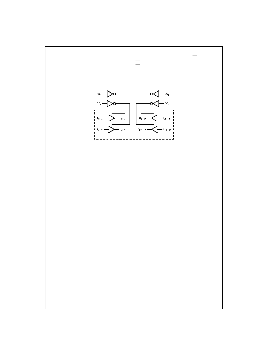
Functional Description
The 74VCX16244 contains sixteen non-inverting buffers
with 3-STATE outputs. The device is nibble (4 bits) con-
trolled with each nibble functioning identically, but indepen-
dent of each other. The control pins may be shorted
together to obtain full 16-bit operation.The 3-STATE out-
puts are controlled by an Output Enable (OE
n
) input. When
OE
n
is LOW, the outputs are in the 2-state mode. When
OE
n
is HIGH, the standard outputs are in the high imped-
ance mode but this does not interfere with entering new
data into the inputs.
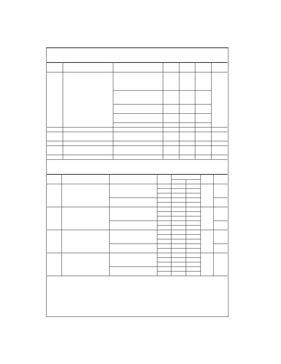
Logic Diagram
www.fairchildsemi.com
4
74VCX16244
Absolute Maximum Ratings
(Note 4)
Recommended Operating
Conditions
(Note 6)
Note 4: The Absolute Maximum Ratings are those values beyond which
the safety of the device cannot be guaranteed. The device should not be
operated at these limits. The parametric values defined in the Electrical
Characteristics tables are not guaranteed at the Absolute Maximum Rat-
ings. The "Recommended Operating Conditions" table will define the condi-
tions for actual device operation.
Note 5: I
O
Absolute Maximum Rating must be observed.
Note 6: Floating or unused inputs must be held HIGH or LOW.
DC Electrical Characteristics
Supply Voltage (V
CC
)
0.5V to
4.6V
DC Input Voltage (V
I
)
0.5V to
4.6V
Output Voltage (V
O
)
Outputs 3-STATED
0.5V to
4.6V
Outputs Active (Note 5)
0.5V to V
CC
0.5V
DC Input Diode Current (I
IK
) V
I
0V
50 mA
DC Output Diode Current (I
OK
)
V
O
0V
50 mA
V
O
!
V
CC
50 mA
DC Output Source/Sink Current
(I
OH
/I
OL
)
r
50 mA
DC V
CC
or GND Current per
Supply Pin (I
CC
or GND)
r
100 mA
Storage Temperature Range (T
STG
)
65
q
C to
150
q
C
Power Supply
Operating
1.2V to 3.6V
Input Voltage
0.3V to
3.6V
Output Voltage (V
O
)
Output in Active States
0.0V to V
CC
Output in 3-State
0.0V to 3.6V
Output Current in I
OH
/I
OL
V
CC
3.0V to 3.6V
r
24 mA
V
CC
2.3V to 2.7V
r
18 mA
V
CC
1.65V to 2.3V
r
6 mA
V
CC
1.4V to 1.6V
r
2 mA
V
CC
1.2V
r
100
P
A
Free Air Operating Temperature (T
A
)
40
q
C to
85
q
C
Minimum Input Edge Rate (
'
t/
'
V)
V
IN
0.8V to 2.0V, V
CC
3.0V
10 ns/V
Symbol
Parameter
Conditions
V
CC
Min
Max
Units
(V)
V
IH
HIGH Level Input Voltage
2.7 - 3.6
2.0
V
2.3 - 2.7
1.6
1.65 - 2.3
0.65
u
V
CC
1.4 - 1.6
0.65
u
V
CC
1.2
0.65 x V
CC
V
IL
LOW Level Input Voltage
2.7 - 3.6
0.8
V
2.3 - 2.7
0.7
1.65 - 2.3
0.35
u
V
CC
1.4 - 1.6
0.35
u
V
CC
1.2
0.05 x V
CC
V
OH
HIGH Level Output Voltage
I
OH
100
P
A
2.7 - 3.6
V
CC
- 0.2
V
I
OH
12 mA
2.7
2.2
I
OH
18 mA
3.0
2.4
I
OH
24 mA
3.0
2.2
I
OH
100
P
A
2.3 - 2.7
V
CC
- 0.2
I
OH
6 mA
2.3
2.0
I
OH
12 mA
2.3
1.8
I
OH
18 mA
2.3
1.7
I
OH
100
P
A
1.65 - 2.3
V
CC
- 0.2
I
OH
6 mA
1.65
1.25
I
OH
100
P
A
1.4 - 1.6
V
CC
- 0.2
I
OH
2 mA
1.4
1.05
I
OH
100
P
A
1.2
V
CC
- 0.2
5
www.fairchildsemi.com
7
4
VC
X16
244
DC Electrical Characteristics
(Continued)
Note 7: Outputs disabled or 3-STATE only.
AC Electrical Characteristics
(Note 8)
Note 8: For C
L
50
P
F, add approximately 300 ps to the AC maximum specification.
Note 9: Skew is defined as the absolute value of the difference between the actual propagation delay for any two separate outputs of the same device. The
specification applies to any outputs switching in the same direction, either HIGH-to-LOW (t
OSHL
) or LOW-to-HIGH (t
OSLH
).
Symbol
Parameter
Conditions
V
CC
Min
Max
Units
(V)
V
OL
LOW Level Output Voltage
I
OL
100
P
A
2.7 - 3.6
0.2
V
I
OL
12 mA
2.7
0.4
I
OL
18 mA
3.0
0.4
I
OL
24 mA
3.0
0.55
I
OL
100
P
A
2.3 - 2.7
0.2
I
OL
12 mA
2.3
0.4
I
OL
18 mA
2.3
0.6
I
OL
100
P
A
1.65 - 2.3
0.2
I
OL
6 mA
1.65
0.3
I
OL
100
P
A
1.4 - 1.6
0.2
I
OL
2 mA
1.4
0.35
I
OL
100
P
A
1.2
0.05
I
I
Input Leakage Current
0
d
V
I
d
3.6V
1.2 - 3.6
r
5.0
P
A
I
OZ
3-STATE Output Leakage
0
d
V
O
d
3.6V
1.2 - 3.6
r
10.0
P
A
V
I
V
IH
or V
IL
I
OFF
I
Power-OFF Leakage Current
0
d
(V
I
, V
O
)
d
3.6V
0
10.0
P
A
I
CC
Quiescent Supply Current
V
I
V
CC
or GND
1.2 - 3.6
20.0
P
A
V
CC
d
(V
I
, V
O
)
d
3.6V (Note 7)
1.2 - 3.6
r
20.0
'
I
CC
Increase in I
CC
per Input
V
IH
V
CC
0.6V
2.7 - 3.6
750
P
A
Symbol
Parameter
Conditions
V
CC
T
A
40
q
C to
85
q
C
Units
Figure
(V)
Min
Max
Number
t
PHL
Propagation Delay
C
L
30 pF, R
L
500
:
3.3
r
0.3
0.8
2.5
ns
Figures
1, 2
t
PLH
2.5
r
0.2
1.0
3.0
1.8
r
0.15
1.5
6.0
C
L
15 pF, R
L
2k
:
1.5
r
0.1
1.0
12.0
Figures
5, 6
1.2
1.5
30.0
t
PZL
Output Enable Time
C
L
30 pF, R
L
500
:
3.3
r
0.3
0.8
3.5
ns
Figures
1, 3, 4
t
PZH
2.5
r
0.2
1.0
4.1
1.8
r
0.15
1.5
8.2
C
L
15 pF, R
L
2k
:
1.5
r
0.1
1.0
16.4
Figures
5, 7, 8
1.2
1.5
41.0
t
PLZ
Output Disable Time
C
L
30 pF, R
L
500
:
3.3
r
0.3
0.8
3.5
ns
Figures
1, 3, 4
t
PHZ
2.5
r
0.2
1.0
3.8
1.8
r
0.15
1.5
6.8
C
L
15 pF, R
L
2k
:
1.5
r
0.1
1.0
13.6
Figures
5, 7, 8
1.2
1.5
34.0
t
OSHL
Output to Output Skew
C
L
30 pF, R
L
500
:
3.3
r
0.3
0.5
ns
t
OSLH
(Note 9)
2.5
r
0.2
0.5
1.8
r
0.15
0.75
C
L
15 pF, R
L
2k
:
1.5
r
0.1
1.5
1.2
1.5