Äîêóìåíòàöèÿ è îïèñàíèÿ www.docs.chipfind.ru
© 2004 Fairchild Semiconductor Corporation
DS500130
www.fairchildsemi.com
March 1998
Revised October 2004
7
4
VC
X16
821 Lo
w
V
o
lt
age 2
0
-Bi
t
D-T
y
pe
Fli
p
-Fl
ops
wit
h
3.
6V T
o
l
e
ran
t
Input
s a
nd Out
puts
74VCX16821
Low Voltage 20-Bit D-Type Flip-Flops
with 3.6V Tolerant Inputs and Outputs
General Description
The VCX16821 contains twenty non-inverting D-type flip-
flops with 3-STATE outputs and is intended for bus oriented
applications.
The 74VCX16821 is designed for low voltage (1.4V to
3.6V) V
CC
applications with I/O compatibility up to 3.6V.
The 74VCX16821 is fabricated with an advanced CMOS
technology to achieve high speed operation while maintain-
ing low CMOS power dissipation.
Features
s
1.4V to 3.6V V
CC
supply operation
s
3.6V tolerant inputs and outputs
s
t
PD
3.5 ns max for 3.0V to 3.6V V
CC
s
Power-off high impedance inputs and outputs
s
Supports live insertion and withdrawal (Note 1)
s
Static Drive (I
OH
/I
OL
)
±
24 mA @ 3.0V V
CC
s
Uses patented noise/EMI reduction circuitry
s
Latch-up performance exceeds 300 mA
s
ESD performance:
Human body model
>
2000V
Machine model
>
200V
Note 1: To ensure the high-impedance state during power up or power
down, OE should be tied to V
CC
through a pull-up resistor; the minimum
value of the resistor is determined by the current-sourcing capability of the
driver.
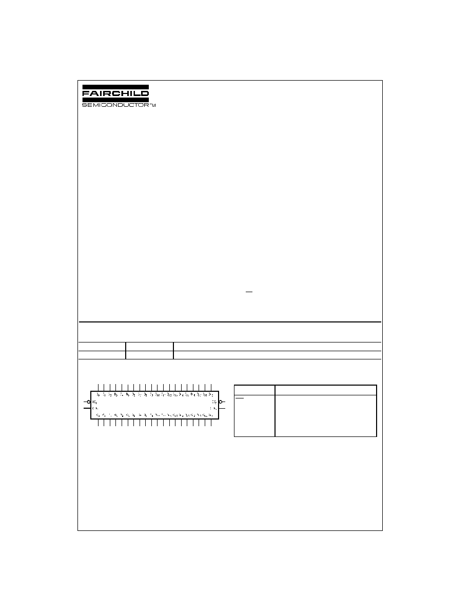
Ordering Code:
Device also available in Tape and Reel. Specify by appending suffix letter "X" to the ordering code.
Logic Symbol
Pin Descriptions
Order Number
Package Number
Package Descriptions
74VCX16821MTD
MTD56
56-Lead Thin Shrink Small Outline Package (TSSOP), JEDEC MO-153, 6.1mm Wide
Pin Names
Description
OE
n
Output Enable Input (Active LOW)
CLK
n
Clock Input
D
0
D
19
Inputs
O
0
O
19
Outputs
www.fairchildsemi.com
2
74VCX16821
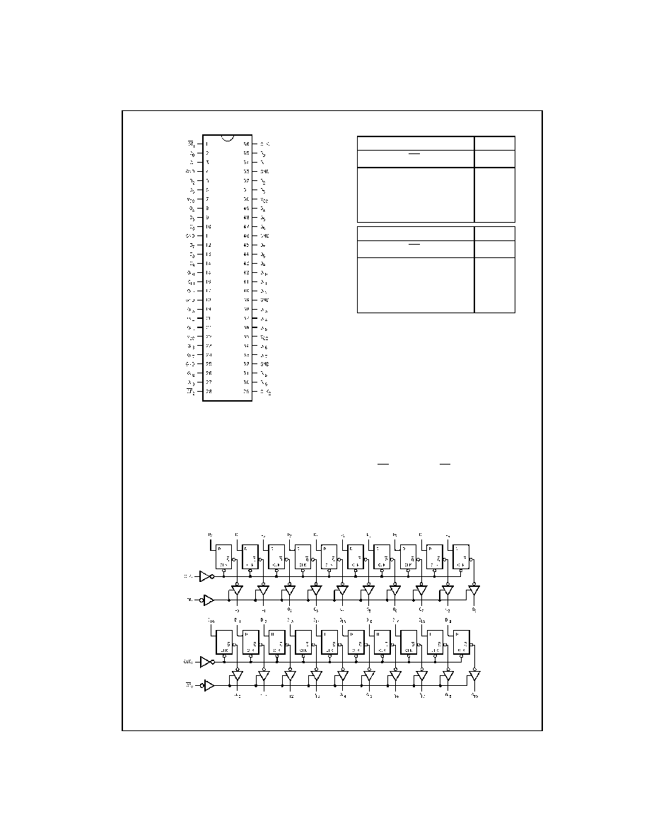
Connection Diagram
Truth Tables
H
=
HIGH Voltage Level
L
=
LOW Voltage Level
X
=
Immaterial (HIGH or LOW, inputs may not float)
Z
=
High Impedance
O
0
=
Previous O
0
before LOW-to-HIGH transition of Clock
=
LOW-to-HIGH transition
Functional Description
The VCX16821 contains twenty D-type flip-flops with
3-STATE standard outputs. The device is byte controlled
with each byte functioning identically, but independent of
each other. Control pins can be shorted together to obtain
full 20-bit operation. The following description applies to
each byte. The twenty flip-flops will store the state of their
individual D-type inputs that meet the setup and hold time
requirements on the LOW-to-HIGH Clock (CLK) transition.
The 3-STATE standard outputs are controlled by the Out-
put Enable (OE
n
) input. When OE
n
is HIGH, the standard
outputs are in the high impedance mode but this does not
interfere with entering new data into the flip-flops.
Logic Diagrams
Please note that this diagram is provided only for the understanding of logic operations and should not be used to estimate propagation delays.
Inputs
Outputs
CLK
1
OE
1
D
0
D
9
O
0
O
9
X
H
X
Z
L
L
L
L
H
H
L or H
L
X
O
0
Inputs
Outputs
CLK
2
OE
2
D
10
D
19
O
10
O
19
X
H
X
Z
L
L
L
L
H
H
L or H
L
X
O
0
3
www.fairchildsemi.com
7
4
VC
X16
821
Absolute Maximum Ratings
(Note 2)
Recommended Operating
Conditions
(Note 4)
Note 2: The Absolute Maximum Ratings are those values beyond which
the safety of the device cannot be guaranteed. The device should not be
operated at these limits. The parametric values defined in the Electrical
Characteristics tables are not guaranteed at the Absolute Maximum Rat-
ings. The "Recommended Operating Conditions" table will define the condi-
tions for actual device operation.
Note 3: I
O
Absolute Maximum Rating must be observed.
Note 4: Floating or unused inputs must be held HIGH or LOW.
DC Electrical Characteristics
Supply Voltage (V
CC
)
-
0.5V to
+
4.6V
DC Input Voltage (V
I
)
-
0.5V to
+
4.6V
Output Voltage (V
O
)
Outputs 3-STATE
-
0.5V to
+
4.6V
Outputs Active (Note 3)
-
0.5V to V
CC
+
0.5V
DC Input Diode Current (I
IK
) V
I
<
0V
-
50 mA
DC Output Diode Current (I
OK
)
V
O
<
0V
-
50 mA
V
O
>
V
CC
+
50 mA
DC Output Source/Sink Current
(I
OH
/I
OL
)
±
50 mA
DC V
CC
or GND Current per
Supply Pin (I
CC
or GND)
±
100 mA
Storage Temperature Range (T
STG
)
-
65
°
C to
+
150
°
C
Power Supply
Operating
1.4V to 3.6V
Input Voltage
-
0.3V to
+
3.6V
Output Voltage (V
O
)
Output in Active States
0V to V
CC
Output in 3-STATE
0.0V to 3.6V
Output Current in I
OH
/I
OL
V
CC
=
3.0V to 3.6V
±
24 mA
V
CC
=
2.3V to 2.7V
±
18 mA
V
CC
=
1.65V to 2.3V
±
6 mA
V
CC
=
1.4V to 1.6V
±
2 mA
Free Air Operating Temperature (T
A
)
-
40
°
C to
+
85
°
C
Minimum Input Edge Rate (
t/
V)
V
IN
=
0.8V to 2.0V, V
CC
=
3.0V
10 ns/V
Symbol
Parameter
Conditions
V
CC
Min
Max
Units
(V)
V
IH
HIGH Level Input Voltage
2.7 - 3.6
2.0
V
2.3 - 2.7
1.6
1.65 - 2.3
0.65 x V
CC
1.4 - 1.6
0.65 x V
CC
V
IL
LOW Level Input Voltage
2.7 - 3.6
0.8
V
2.3 - 2.7
0.7
1.65 - 2.3
0.35 x V
CC
1.4 - 1.6
0.35 x V
CC
V
OH
HIGH Level Output Voltage
I
OH
=
-
100
µ
A 2.7
-
3.6
V
CC
- 0.2
V
I
OH
=
-
12 mA
2.7
2.2
I
OH
=
-
18 mA
3.0
2.4
I
OH
=
-
24 mA
3.0
2.2
I
OH
=
-
100
µ
A 2.3
-
2.7
V
CC
- 0.2
I
OH
=
-
6 mA
2.3
2.0
I
OH
=
-
12 mA
2.3
1.8
I
OH
=
-
18 mA
2.3
1.7
I
OH
=
-
100
µ
A
1.65 - 2.3
V
CC
- 0.2
I
OH
=
-
6 mA
1.65
1.25
I
OH
=
-
100
µ
A 1.4
-
1.6
V
CC
- 0.2
I
OH
=
-
12 mA
1.4
1.05
www.fairchildsemi.com
4
74VCX16821
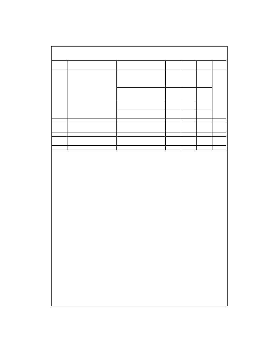
DC Electrical Characteristics
(Continued)
Note 5: Outputs disabled or 3-STATE only.
Symbol
Parameter
Conditions
V
CC
Min
Max
Units
(V)
V
OL
LOW Level Output Voltage
I
OL
=
100
µ
A
2.7 - 3.6
0.2
V
I
OL
=
12 mA
2.7
0.4
I
OL
=
18 mA
3.0
0.4
I
OL
=
24 mA
3.0
0.55
I
OL
=
100
µ
A
2.3 - 2.7
0.2
I
OL
=
6 mA
2.3
0.4
I
OL
=
12 mA
2.3
0.6
I
OL
=
100
µ
A
1.65 - 2.3
0.2
I
OL
=
6 mA
1.65
0.3
I
OL
=
100
µ
A
1.4 - 1.6
0.2
I
OL
=
2 mA
1.4
0.35
I
I
Input Leakage Current
0
V
I
3.6V
1.4 - 3.6
±
5.0
µ
A
I
OZ
3-STATE Output Leakage
0
V
O
3.6V
1.4 - 3.6
±
10
µ
A
V
I
=
V
IH
or V
IL
I
OFF
Power-OFF Leakage Current
0
(V
I
, V
O
)
3.6V
0
10
µ
A
I
CC
Quiescent Supply Current
V
I
=
V
CC
or GND
1.4 - 3.6
20
µ
A
V
CC
(V
I
, V
O
)
3.6V (Note 5)
1.4 - 3.6
±
20
I
CC
Increase in I
CC
per Input
V
IH
=
V
CC
-
0.6V
2.7 - 3.6
750
µ
A
5
www.fairchildsemi.com
7
4
VC
X16
821
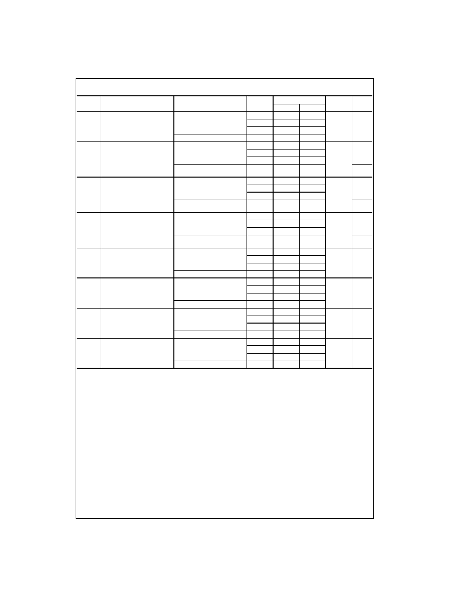
AC Electrical Characteristics
(Note 6)
Note 6: For C
L
=
50
P
F, add approximately 300 ps to the AC maximum specification.
Note 7: Skew is defined as the absolute value of the difference between the actual propagation delay for any two separate outputs of the same device. The
specification applies to any outputs switching in the same direction, either HIGH-to-LOW (t
OSHL
) or LOW-to-HIGH (t
OSLH
).
Symbol
Parameter
Conditions
V
CC
T
A
=
-
40
°
C to
+
85
°
C
Units
Figure
(V)
Min
Max
Number
f
MAX
Maximum Clock Frequency
C
L
=
30 pF, R
L
=
500
3.3
±
0.3
250
MHz
2.5
±
0.2
200
1.8
±
0.15
100
C
L
=
15 pF, R
L
=
500
1.5
±
0.1
80.0
t
PHL
Propagation Delay
C
L
=
30 pF, R
L
=
500
3.3
±
0.3
0.8
3.5
ns
Figures
1, 2
t
PLH
2.5
±
0.2
1.0
4.4
1.8
±
0.15
1.5
8.8
C
L
=
15 pF, R
L
=
500
1.5
±
0.1
1.0
17.6
Figures
7, 8
t
PZL
Output Enable Time
C
L
=
30 pF, R
L
=
500
3.3
±
0.3
0.8
3.7
ns
Figures
1, 3, 4
t
PZH
2.5
±
0.2
1.0
4.7
1.8
±
0.15
1.5
9.8
C
L
=
15 pF, R
L
=
500
1.5
±
0.1
1.0
19.6
Figures
7, 9, 10
t
PLZ
Output Disable Time
C
L
=
30 pF, R
L
=
500
3.3
±
0.3
0.8
3.7
ns
Figures
1, 3, 4
t
PHZ
2.5
±
0.2
1.0
4.2
1.8
±
0.15
1.5
7.6
C
L
=
15 pF, R
L
=
500
1.5
±
0.1
1.0
15.2
Figures
7, 9, 10
t
S
Setup Time
C
L
=
30 pF, R
L
=
500
3.3
±
0.3
1.5
ns
Figure 6
2.5
±
0.2
1.5
1.8
±
0.15
2.5
C
L
=
15 pF, R
L
=
500
1.5
±
0.1
3.0
t
H
Hold Time
C
L
=
30 pF, R
L
=
500
3.3
±
0.3
1.0
ns
Figure 6
2.5
±
0.2
1.0
1.8
±
0.15
1.0
C
L
=
15 pF, R
L
=
500
1.5
±
0.1
2.0
t
W
Pulse Width
C
L
=
30 pF, R
L
=
500
3.3
±
0.3
1.5
ns
Figure 5
2.5
±
0.2
1.5
1.8
±
0.15
4.0
C
L
=
15 pF, R
L
=
500
1.5
±
0.1
4.0
t
OSHL
Output to Output Skew
C
L
=
30 pF, R
L
=
500
3.3
±
0.3
0.5
ns
t
OSLH
(Note 7)
2.5
±
0.2
0.5
1.8
±
0.15
0.75
C
L
=
15 pF, R
L
=
500
1.5
±
0.1
1.5