
© 2000 Fairchild Semiconductor Corporation
DS500173
www.fairchildsemi.com
October 1998
Revised April 2000
7
4
VC
X16
835
Lo
w
V
o
lt
age
1
8
-Bi
t
Univer
sal Bus Driv
er w
i
th 3.
6V
T
o
l
e
rant
I
nput
s
and Output
s
74VCX16835
Low Voltage 18-Bit Universal Bus Driver
with 3.6V Tolerant Inputs and Outputs
General Description
The VCX16835 low voltage 18-bit universal bus driver
combines D-type latches and D-type flip-flops to allow data
flow in transparent, latched and clocked modes.
Data flow is controlled by output-enable (OE), latch-enable
(LE), and clock (CLK) inputs. The device operates in
Transparent Mode when LE is held HIGH. The device
operates in clocked mode when LE is LOW and CLK is tog-
gled. Data transfers from the Inputs (I
n
) to Ouputs (O
n
) on a
Positive Edge Transition of the Clock. When OE is LOW,
the output data is enabled. When OE is HIGH the output
port is in a high impedance state.
The 74VCX16835 is designed for low voltage (1.65V to
3.6V) V
CC
applications with I/O capability up to 3.6V.
The 74VCX16835 is fabricated with an advanced CMOS
technology to achieve high speed operation while maintain-
ing low CMOS power dissipation.
Features
s
Compatible with PC100 DIMM module specifications
s
1.65V≠3.6V V
CC
specifications provided
s
3.6V tolerant inputs and outputs
s
t
PD
(CP to O
n
)
4.2ns max for 3.0V to 3.6V V
CC
5.2ns max for 2.3V to 2.7V V
CC
9.2ns max for 1.65V to 1.95V V
CC
s
Power-down high impedance inputs and outputs
s
Supports live insertion/withdrawal (Note 1)
s
Static Drive (I
OH
/I
OL
)
±
24mA @ 3.0V
±
18mA @ 2.3V
±
6mA @
1.65V
s
Latchup performance exceeds 300 mA
s
ESD performance:
Human body model
>
2000V
Machine model
>
200V
Note 1: To ensure the high-impedance state during power up or power
down, OE should be tied to V
CC
(OE to GND) through a pulldown resistor;
the minimum value of the resistor is determined by the current sourcing
capability of the driver.
Ordering Code:
Devices also available in Tape and Reel. Specify by appending the suffix letter "X" to the ordering code.
Order Number
Package Number
Package Description
74VCX16835MTD
MTD56
56-Lead Thin Shrink Small Outline Package (TSSOP), JEDEC MO-153, 6.1mm Wide
www.fairchildsemi.com
2
74VCX16835
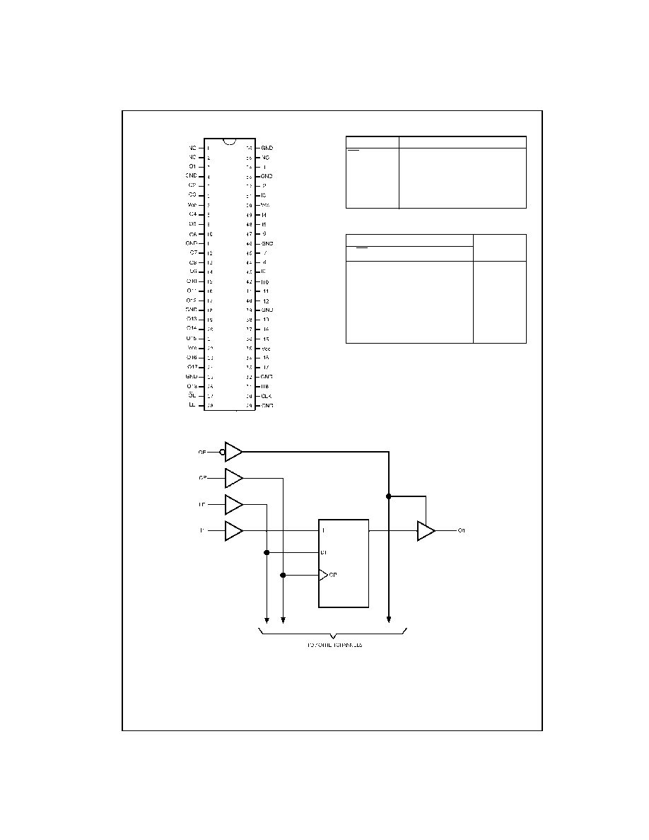
Connection Diagram
Pin Descriptions
Function Table
H
=
HIGH Voltage Level
L
=
LOW Level Voltage
X
=
Immaterial (HIGH or LOW, Inputs may not float)
Z
=
High Impedance
Note 2: Output level before the indicated steady-state input conditions
were established provided that CP was HIGH before LE went LOW.
Note 3: Output level before the indicated steady-state input conditions
were established.
Logic Diagram
Pin Names
Description
OE
Output Enable Input (Active LOW)
LE
Latch Enable Input
CP
Clock Input
I
1
- I
18
Data Inputs
O
1
- O
18
3-STATE Outputs
Inputs
Outputs
OE
LE
CP
I
n
O
n
H
X
X
X
Z
L
H
X
L
L
L
H
X
H
H
L
L
L
L
L
L
H
H
L
L
H
X
O
0
(Note 2)
L
L
L
X
O
0
(Note 3)
3
www.fairchildsemi.com
7
4
VC
X16
835
Absolute Maximum Ratings
(Note 4)
Recommended Operating
Conditions
(Note 6)
Note 4: The "Absolute Maximum Ratings" are those values beyond which
the safety of the device cannot be guaranteed. The device should not be
operated at these limits. The parametric values defined in the Electrical
Characteristics tables are not guaranteed at the Absolute Maximum Rat-
ings. The Recommended Operating Conditions tables will define the condi-
tions for actual device operation.
Note 5: I
O
Absolute Maximum Rating must be observed.
Note 6: Floating or unused pin (inputs or I/O's) must be held HIGH or LOW.
DC Electrical Characteristics (2.7V
<
V
CC
3.6V)
Note 7: Outputs disabled or 3-STATE only.
Supply Voltage (V
CC
)
-
0.5V to
+
4.6V
DC Input Voltage (V
I
)
-
0.5V to
+
4.6V
Output Voltage (V
O
)
Outputs 3-STATE
-
0.5V to
+
4.6V
Outputs Active (Note 5)
-
0.5 to V
CC
+
0.5V
DC Input Diode Current (I
IK
) V
I
<
0V
-
50 mA
DC Output Diode Current (I
OK
)
V
O
<
0V
-
50 mA
V
O
>
V
CC
+
50 mA
DC Output Source/Sink Current
(I
OH
/I
OL
)
±
50 mA
DC V
CC
or Ground Current per
Supply Pin (I
CC
or Ground)
±
100 mA
Storage Temperature Range (T
STG
)
-
65
∞
C to
+
150
∞
C
Power Supply
Operating
1.65V to 3.6V
Data Retention Only
1.2V to 3.6V
Input Voltage
-
0.3V to 3.6V
Output Voltage (V
O
)
Output in Active States
0V to V
CC
Output in 3-STATE
0.0V to 3.6V
Output Current in I
OH
/I
OL
V
CC
=
3.0V to 3.6V
±
24 mA
V
CC
=
2.3V to 2.7V
±
18 mA
V
CC
=
1.65V to 2.3V
±
6 mA
Free Air Operating Temperature (T
A
)
-
40
∞
C to
+
85
∞
C
Minimum Input Edge Rate (
t/
V)
V
IN
=
0.8V to 2.0V, V
CC
=
3.0V
10 ns/V
Symbol
Parameter
Conditions
V
CC
Min
Max
Units
(V)
V
IH
HIGH Level Input Voltage
2.7≠3.6
2.0
V
V
IL
LOW Level Input Voltage
2.7≠3.6
0.8
V
V
OH
HIGH Level Output Voltage
I
OH
=
-
100
µ
A
2.7≠3.6
V
CC
-
0.2
I
OH
=
-
12 mA
2.7
2.2
V
I
OH
=
-
18 mA
3.0
2.4
I
OH
=
-
24 mA
3.0
2.2
V
OL
LOW Level Output Voltage
I
OL
=
100
µ
A
2.7≠3.6
0.2
I
OL
=
12 mA
2.7
0.4
V
I
OL
=
18 mA
3.0
0.4
I
OL
=
24 mA
3.0
0.55
I
I
Input Leakage Current
0V
V
I
3.6V
2.7≠3.6
±
5.0
µ
A
I
OZ
3-STATE Output Leakage
0V
V
O
3.6V
2.7≠3.6
±
10
µ
A
V
I
=
V
IH
or V
IL
I
OFF
Power Off Leakage Current
0V
(V
I
, V
O
)
3.6V
0
10
µ
A
I
CC
Quiescent Supply Current
V
I
=
V
CC
or GND
2.7≠3.6
20
µ
A
V
CC
(V
I
, V
O
)
3.6V (Note 7)
2.7≠3.6
±
20
I
CC
Increase in I
CC
per Input
V
IH
=
V
CC
-
0.6V
2.7≠3.6
750
µ
A

www.fairchildsemi.com
4
74VCX16835
DC Electrical Characteristics (2.3V
V
CC
2.7V)
Note 8: Outputs disabled or 3-STATE only.
DC Electrical Characteristics (1.65V
V
CC
<
2.3V)
Note 9: Outputs disabled or 3-STATE only.
Symbol
Parameter
Conditions
V
CC
Min
Max
Units
(V)
V
IH
HIGH Level Input Voltage
2.3 - 2.7
1.6
V
V
IL
LOW Level Input Voltage
2.3 - 2.7
0.7
V
V
OH
HIGH Level Output Voltage
I
OH
=
-
100
µ
A
2.3 -2.7
V
CC
-
0.2
V
I
OH
=
-
6 mA
2.3
2.0
I
OH
=
-
12 mA
2.3
1.8
I
OH
=
-
18 mA
2.3
1.7
V
OL
LOW Level Output Voltage
I
OL
=
100
µ
A
2.3 - 2.7
0.2
I
OL
=
12mA
2.3
0.4
V
I
OL
=
18 mA
2.3
0.6
I
I
Input Leakage Current
0
V
I
3.6V
2.3 - 2.7
±
5.0
µ
A
I
OZ
3-STATE Output Leakage
0
V
O
3.6V
2.3 - 2.7
±
10
µ
A
V
I
=
V
IH
or V
IL
I
OFF
Power Off Leakage Current
0
(V
I
, V
O
)
3.6V
0
10
µ
A
I
CC
Quiescent Supply Current
V
I
=
V
CC
or GND
2.3 - 2.7
20
µ
A
V
CC
(V
I
, V
O
)
3.6V (Note 8)
2.3 - 2.7
±
20
Symbol
Parameter
Conditions
V
CC
Min
Max
Units
(V)
V
IH
HIGH Level Input Voltage
1.65 - 2.3
0.65
◊
V
CC
V
V
IL
LOW Level Input Voltage
1.65 - 2.3
0.35
◊
V
CC
V
V
OH
HIGH Level Output Voltage
I
OH
=
-
100
µ
A
1.65 - 2.3
V
CC
-
0.2
V
I
OH
=
-
6 mA
1.65
1.25
V
OL
LOW Level Output Voltage
I
OL
=
100
µ
A
1.65 - 2.3
0.2
V
I
OL
=
6mA
1.65
0.3
I
I
Input Leakage Current
0
V
I
3.6V
1.65 - 2.3
±
5.0
µ
A
I
OZ
3-STATE Output Leakage
0
V
O
3.6V
1.65 - 2.3
±
10
µ
A
V
I
=
V
IH
or V
IL
I
OFF
Power Off Leakage Current
0
(V
I
, V
O
)
3.6V
0
10
µ
A
I
CC
Quiescent Supply Current
V
I
=
V
CC
or GND
1.65 - 2.3
20
µ
A
V
CC
(V
I
, V
O
)
3.6V (Note 9)
1.65 - 2.3
±
20
5
www.fairchildsemi.com
7
4
VC
X16
835
AC Electrical Characteristics
(Note 10)
Note 10: For CL
=
50pF, add approximately 300ps to the AC maximum specification.
Note 11: Skew is defined as the absolute value of the difference between the actual propagation delay for any two separate outputs of the same device. The
specification applies to any outputs switching in the same direction, either HIGH-to-LOW (t
OSHL
) or LOW-to-HIGH (t
OSLH
).
AC Electrical Characteristics Over Load
(Note 12)
Note 12: This parameter is guaranteed by characterization but not tested.
Note 13: SSO = Simultaneous Switching Output. Any output combination of LOW-to-HIGH and/or HIGH-to-LOW transition.
Dynamic Switching Characteristics
Symbol
Parameter
T
A
=
-
40
∞
C to
+
85
∞
C, C
L
=
30 pF, R
L
=
500
Units
V
CC
=
3.3V
±
0.3V
V
CC
=
2.5
±
0.2V
V
CC
=
1.8
±
0.15V
Min
Max
Min
Max
Min
Max
f
MAX
Maximum Clock Frequency
250
200
100
MHz
t
PHL
, Propagation
Delay
0.6
3.3
0.8
4.2
1.5
8.4
ns
t
PLH
Bus to Bus
t
PHL
, Propagation
Delay
1.4
4.2
1.5
5.2
2.0
9.2
ns
t
PLH
Clock to Bus
t
PHL
, Propagation
Delay
0.6
3.8
0.8
4.9
1.5
9.8
ns
t
PLH
LE to Bus
t
PZL
, t
PZH
Output Enable Time
0.6
3.8
0.8
4.9
1.5
9.8
ns
t
PLZ
, t
PHZ
Output Disable Time
0.6
3.9
0.8
4.5
1.5
7.6
ns
t
S
Setup Time
1.5
1.5
2.5
ns
t
H
Hold Time
0.7
0.7
1.0
ns
t
W
Pulse Width
1.5
1.5
4.0
ns
t
OSHL
Output to Output Skew
0.5
0.5
0.75
ns
t
OSLH
(Note 11)
Symbol
Parameter
T
A
=
-
0
∞
C to
+
85
∞
C, R
L
=
500
V
CC
=
3.3V
±
0.15V
Units
C
L
=
0 pF
C
L
=
50 pF
Min
Max
Min
Max
t
PHL
, t
PLH
Prop Delay Bus to Bus
0.7
2.1
1.0
3.6
ns
t
PHL
, t
PLH
Prop Delay Clock to Bus
1.5
3.0
1.7
4.5
ns
t
PHL
, t
PLH
Prop Delay LE to Bus
0.7
2.6
1.0
4.1
ns
t
PZL
, t
PZH
Output Enable Time
0.7
2.6
1.0
4.1
ns
t
PLZ
, t
PHZ
Output Disable Time
0.7
2.7
1.0
4.2
ns
t
PHL
, t
PLH
SSO Prop Delay Clock to Bus (Note 13)
1.5
3.3
ns
t
S
Setup Time
1.5
1.5
ns
t
H
Hold Time
0.7
0.7
ns
Symbol
Parameter
Conditions
V
CC
T
A
=+
25
∞
C
Units
(V)
Typical
V
OLP
Quiet Output Dynamic Peak V
OL
C
L
=
30 pF, V
IH
=
V
CC
, V
IL
=
0V
1.8
0.35
2.5
0.7
V
3.3
0.9
V
OLV
Quiet Output Dynamic Valley V
OL
C
L
=
30 pF, V
IH
=
V
CC
, V
IL
=
0V
1.8
-
0.35
2.5
-
0.7
V
3.3
-
0.9
V
OHV
Quiet Output Dynamic Valley V
OH
C
L
=
30 pF, V
IH
=
V
CC
, V
IL
=
0V
1.8
1.3
2.5
1.7
V
3.3
2.0