© 2000 Fairchild Semiconductor Corporation
DS500034
www.fairchildsemi.com
July 1997
Revised July 2000
7
4
VC
X16
838 Lo
w
V
o
lt
age 1
6
-Bi
t
Select
abl
e
Regi
ste
r
/
B
uf
fe
r
w
i
th
3.
6V T
o
l
e
rant
I
nput
s and
Output
s
74VCX16838
Low Voltage 16-Bit Selectable Register/Buffer
with 3.6V Tolerant Inputs and Outputs
General Description
The VCX16838 contains sixteen non-inverting selectable
buffered or registered paths. The device can be configured
to operate in a registered, or flow through buffer mode by
utilizing the register enable (REGE) and Clock (CP) sig-
nals. The device operates in a 16-bit word wide mode. All
outputs can be placed into 3-State through use of the OE
Pin. These devices are ideally suited for buffered or regis-
tered 168 pin and 200 pin SDRAM DIMM memory mod-
ules.
The 74VCX16838 is designed for low voltage (1.65V to
3.6V) V
CC
applications with I/O compatibility up to 3.6V.
The 74VCX16838 is fabricated with an advanced CMOS
technology to achieve high speed operation while maintain-
ing low CMOS power dissipation.
Features
s
Compatible with PC100 and PC133 DIMM module
specifications
s
1.65V≠3.6V V
CC
supply operation
s
3.6V tolerant inputs and outputs
s
t
PD
(CP to O
n
)
3.0 ns max for 3.0V to 3.6V V
CC
4.0 ns max for 2.3V to 2.7V V
CC
8.0 ns max for 1.65V to 1.95V V
CC
s
Power-off high impedance inputs and outputs
s
Supports live insertion and withdrawal (Note 1)
s
Static Drive (I
OH
/I
OL
)
±
24 mA @ 3.0V V
CC
±
18 mA @ 2.3V V
CC
±
6 mA @ 1.65V V
CC
s
Uses patented noise/EMI reduction circuitry
s
Ideal for SDRAM DIMM modules
s
Latch-up performance exceeds 300 mA
s
ESD performance:
Human body model
>
2000V
Machine model
>
200V
Note 1: To ensure the high-impedance state during power up or power
down, OE should be tied to V
CC
through a pull-up resistor; the minimum
value of the resistor is determined by the current-sourcing capability of the
driver.
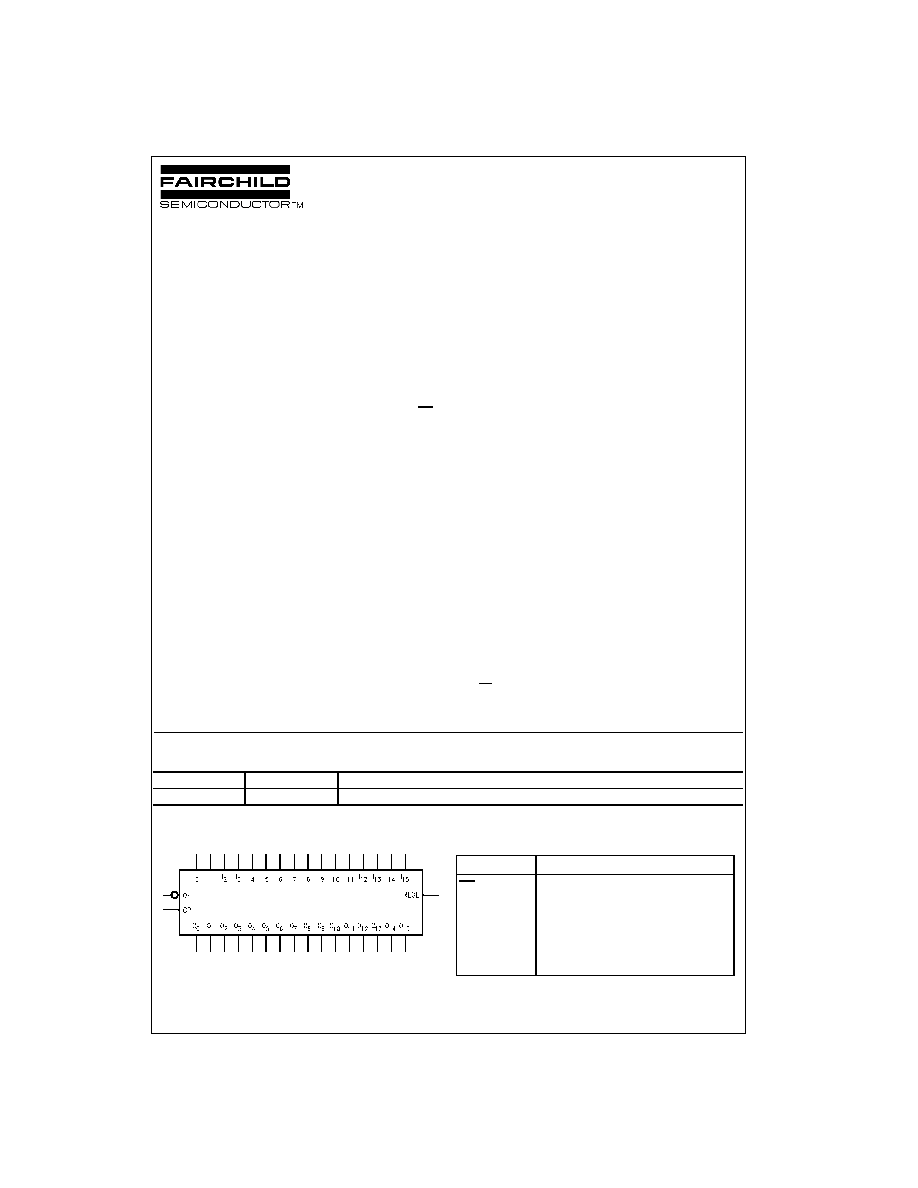
Ordering Code:
Devices also available in Tape and Reel. Specify by appending suffix letter "X" to the ordering code.
Logic Symbol
Pin Descriptions
Order Number
Package Number
Package Description
74VCX16838MTD
MTD48
48-Lead Thin Shrink Small Outline Package (TSSOP), JEDEC MO-153, 6.1mm Wide
Pin Names
Description
OE
Output Enable Input (Active LOW)
I
0
≠I
15
Inputs
O
0
≠O
15
Outputs
CP
Clock Pulse Input
REGE
Register Enable Input
www.fairchildsemi.com
2
74VCX16838
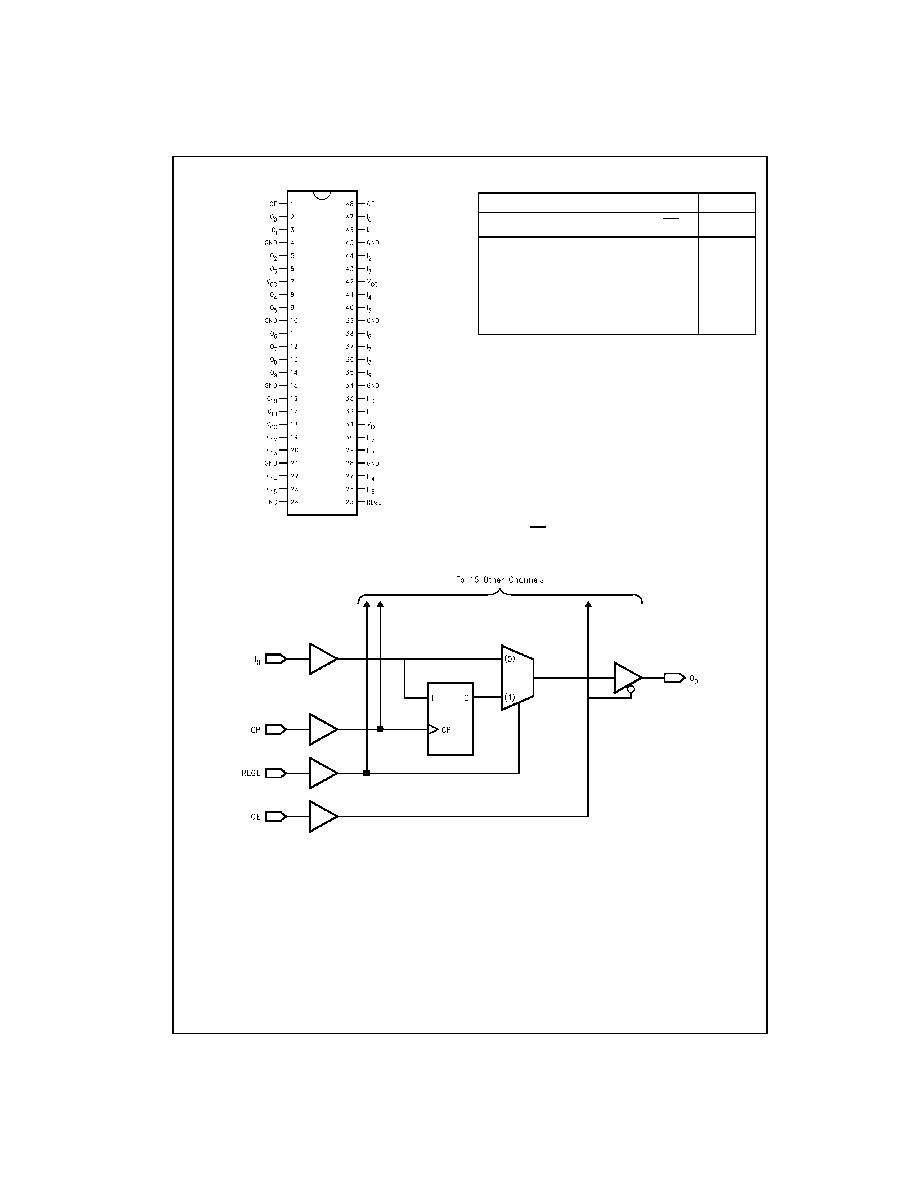
Connection Diagram
Truth Table
H
=
HIGH Voltage Level
L
=
LOW Voltage Level
X
=
Immaterial (HIGH or LOW, inputs may not float)
Z
=
High Impedance
Functional Description
The 74VCX16838 consists of sixteen selectable non-
inverting buffers or registers with word wide controls. Mode
functionality is selected through operation of the CP and
REGE pin as shown by the truth table. When REGE is held
at a logic "1" the device operates as a 16-bit register. Data
is transferred from I
n
to O
n
on the rising edge of the CP pin.
When the REGE pin is held at a logic "0" the device oper-
ates in a flow through mode and data propagates directly
from the I to the O outputs. All outputs can be 3-STATE by
holding the OE pin at a logic "1."
Logic Diagram
Inputs
Outputs
CP
REGE
I
n
OE
O
n
H
H
L
H
H
L
L
L
X
L
H
L
H
X
L
L
L
L
X
X
X
H
Z

3
www.fairchildsemi.com
7
4
VC
X16
838
Absolute Maximum Ratings
(Note 2)
Recommended Operating
Conditions
(Note 4)
Note 2: The Absolute Maximum Ratings are those values beyond which
the safety of the device cannot be guaranteed. The device should not be
operated at these limits. The parametric values defined in the Electrical
Characteristics tables are not guaranteed at the Absolute Maximum Rat-
ings. The "Recommended Operating Conditions" table will define the condi-
tions for actual device operation.
Note 3: I
O
Absolute Maximum Rating must be observed.
Note 4: Floating or unused inputs must be held HIGH or LOW.
DC Electrical Characteristics (2.7V
<
V
CC
3.6V)
Note 5: Outputs disabled or 3-STATE only.
Supply Voltage (V
CC
)
-
0.5V to
+
4.6V
DC Input Voltage (V
I
)
-
0.5V to
+
4.6V
Output Voltage (V
O
)
Outputs 3-STATE
-
0.5V to
+
4.6V
Outputs Active (Note 3)
-
0.5V to V
CC
+
0.5V
DC Input Diode Current (I
IK
) V
I
<
0V
-
50 mA
DC Output Diode Current (I
OK
)
V
O
<
0V
-
50 mA
V
O
>
V
CC
+
50 mA
DC Output Source/Sink Current
(I
OH
/I
OL
)
±
50 mA
DC V
CC
or GND Current per
Supply Pin (I
CC
or GND)
±
100 mA
Storage Temperature Range (T
STG
)
-
65
∞
C to
+
150
∞
C
Power Supply
Operating
1.65V to 3.6V
Data Retention Only
1.2V to 3.6V
Input Voltage
-
0.3V to
+
3.6V
Output Voltage (V
O
)
Output in Active States
0V to V
CC
Output in "OFF" State
0.0V to 3.6V
Output Current in I
OH
/I
OL
V
CC
=
3.0V to 3.6V
±
24 mA
V
CC
=
2.3V to 2.7V
±
18 mA
V
CC
=
1.65V to 2.3V
±
6 mA
Free Air Operating Temperature (T
A
)
-
40
∞
C to
+
85
∞
C
Minimum Input Edge Rate (
t/
V)
V
IN
=
0.8V to 2.0V, V
CC
=
3.0V
10 ns/V
Symbol
Parameter
Conditions
V
CC
(V)
Min
Max
Units
V
IH
HIGH Level Input Voltage
2.7≠3.6
2.0
V
V
IL
LOW Level Input Voltage
2.7≠3.6
0.8
V
V
OH
HIGH Level Output Voltage
I
OH
=
-
100
µ
A
2.7≠3.6
V
CC
-
0.2
V
I
OH
=
-
12 mA
2.7
2.2
V
I
OH
=
-
18 mA
3.0
2.4
V
I
OH
=
-
24 mA
3.0
2.2
V
V
OL
LOW Level Output Voltage
I
OL
=
100
µ
A
2.7≠3.6
0.2
V
I
OL
=
12 mA
2.7
0.4
V
I
OL
=
18 mA
3.0
0.4
V
I
OL
=
24 mA
3.0
0.55
V
I
I
Input Leakage Current
0
V
I
3.6V
2.7≠3.6
±
5.0
µ
A
I
OZ
3-STATE Output Leakage
0
V
O
3.6V
2.7≠3.6
±
10
µ
A
V
I
=
V
IH
or V
IL
I
OFF
Power-OFF Leakage Current
0
(V
I
, V
O
)
3.6V
0
10
µ
A
I
CC
Quiescent Supply Current
V
I
=
V
CC
or GND
2.7≠3.6
20
µ
A
V
CC
(V
I
, V
O
)
3.6V (Note 5)
2.7≠3.6
±
20
µ
A
I
CC
Increase in I
CC
per Input
V
IH
=
V
CC
-
0.6V
2.7≠3.6
750
µ
A
www.fairchildsemi.com
4
74VCX16838
DC Electrical Characteristics (2.3V
V
CC
2.7V)
Note 6: Outputs disabled or 3-STATE only.
DC Electrical Characteristics (1.65V
V
CC
<
2.3V)
Note 7: Outputs disabled or 3-STATE only.
Symbol
Parameter
Conditions
V
CC
(V)
Min
Max
Units
V
IH
HIGH Level Input Voltage
2.3≠2.7
1.6
V
V
IL
LOW Level Input Voltage
2.3≠2.7
0.7
V
V
OH
HIGH Level Output Voltage
I
OH
=
-
100
µ
A
2.3≠2.7
V
CC
-
0.2
V
I
OH
=
-
6 mA
2.3
2.0
V
I
OH
=
-
12 mA
2.3
1.8
V
I
OH
=
-
18 mA
2.3
1.7
V
V
OL
LOW Level Output Voltage
I
OL
=
100
µ
A
2.3≠2.7
0.2
V
I
OL
=
12 mA
2.3
0.4
V
I
OL
=
18 mA
2.3
0.6
V
I
I
Input Leakage Current
0
V
I
3.6V
2.3≠2.7
±
5.0
µ
A
I
OZ
3-STATE Output Leakage
0
V
O
3.6V
2.3≠2.7
±
10
µ
A
V
I
=
V
IH
or V
IL
I
OFF
Power-OFF Leakage Current
0
(V
I
, V
O
)
3.6V
0
10
µ
A
I
CC
Quiescent Supply Current
V
I
=
V
CC
or GND
2.3≠2.7
20
µ
A
V
CC
(V
I
, V
O
)
3.6V (Note 6)
2.3≠2.7
±
20
µ
A
Symbol
Parameter
Conditions
V
CC
(V)
Min
Max
Units
V
IH
HIGH Level Input Voltage
1.65 - 2.3
0.65
◊
V
CC
V
V
IL
LOW Level Input Voltage
1.65 - 2.3
0.35
◊
V
CC
V
V
OH
HIGH Level Output Voltage
I
OH
=
-
100
µ
A
1.65 - 2.3
V
CC
-
0.2
V
I
OH
=
-
6 mA
1.65
1.25
V
V
OL
LOW Level Output Voltage
I
OL
=
100
µ
A
1.65 - 2.3
0.2
V
I
OL
=
6 mA
1.65
0.3
V
I
I
Input Leakage Current
0
V
I
3.6V
1.65 - 2.3
±
5.0
µ
A
I
OZ
3-STATE Output Leakage
0
V
O
3.6V
1.65 - 2.3
±
10
µ
A
V
I
=
V
IH
or V
IL
I
OFF
Power-OFF Leakage Current
0
(V
I
, V
O
)
3.6V
0
10
µ
A
I
CC
Quiescent Supply Current
V
I
=
V
CC
or GND
1.65 - 2.3
20
µ
A
V
CC
(V
I
, V
O
)
3.6V (Note 7)
1.65 - 2.3
±
20
µ
A

5
www.fairchildsemi.com
7
4
VC
X16
838
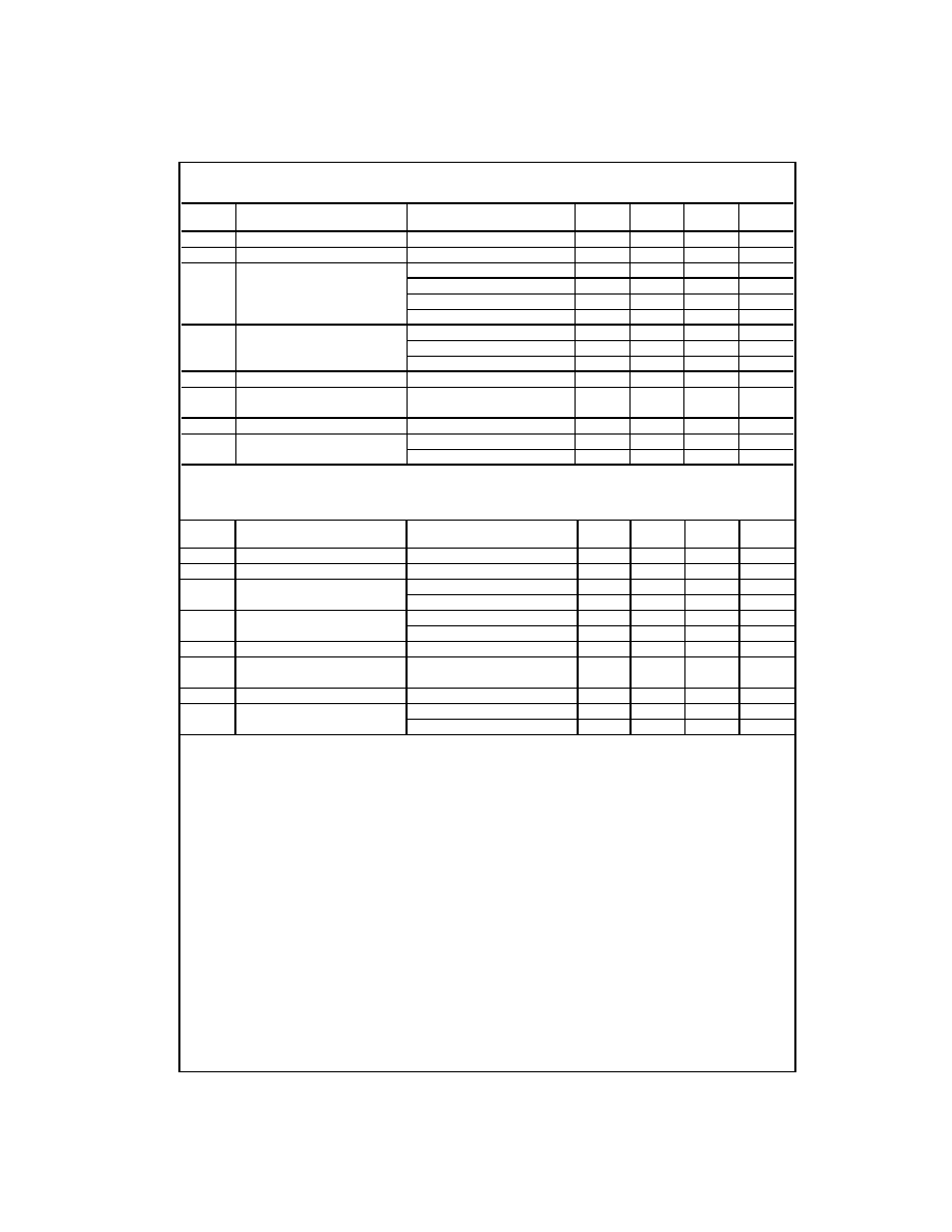
AC Electrical Characteristics
(Note 8)
Note 8: For C
L
=
50
P
F, add approximately 300 ps to the AC maximum specification.
Note 9: Skew is defined as the absolute value of the difference between the actual propagation delay for any two separate outputs of the same device. The
specification applies to any outputs switching in the same direction, either HIGH-to-LOW (t
OSHL
) or LOW-to-HIGH (t
OSLH
).
Extended AC Electrical Characteristics
(Note 10)
Note 10: This parameter is guaranteed by characterization but not tested.
Dynamic Switching Characteristics
Capacitance
Symbol
Parameter
T
A
=
-
40
∞
C to
+
85
∞
C, C
L
=
30 pF, R
L
=
500
Units
V
CC
=
3.3V
±
0.3V
V
CC
=
2.5V
±
0.2V
V
CC
=
1.8V
±
0.15V
Min
Max
Min
Max
Min
Max
f
MAX
Maximum Clock Frequency
250
200
100
MHz
t
PHL
, t
PLH
Prop Delay I
n
to O
n
(REGE
=
0)
0.8
2.5
1.0
3.5
1.5
7.0
ns
t
PHL
, t
PLH
Prop Delay CP to O
n
(REGE
=
1)
0.8
3.0
1.0
4.0
1.5
8.0
ns
t
PHL
, t
PLH
Prop Delay REGE to O
n
0.8
3.0
1.0
4.0
1.5
8.0
ns
t
PZL
, t
PZH
Output Enable Time
0.8
3.5
1.0
4.7
1.5
9.4
ns
t
PLZ
, t
PHZ
Output Disable Time
0.8
3.5
1.0
3.9
1.5
7.0
ns
t
S
Setup Time
1.0
1.0
2.5
ns
t
H
Hold Time
0.7
0.7
1.0
ns
t
W
Pulse Width
1.5
1.5
4.0
ns
t
OSHL
Output to Output Skew
(Note 9)
0.5
0.5
0.75
ns
t
OSLH
Symbol
Parameter
T
A
=
-
0
∞
C to
+
85
∞
C, R
L
=
500
V
CC
=
3.3V
±
0.3V
Units
C
L
=
50 pF
Min
Max
t
PHL
, t
PLH
Prop Delay I
n
to O
n
(REGE
=
0)
1.0
2.8
ns
t
PHL
, t
PLH
Prop Delay CP to O
n
(REGE
=
1)
1.4
3.3
ns
t
PHL
, t
PLH
Prop Delay REGE to O
n
1.0
3.3
ns
t
PZL
, t
PZH
Output Enable Time
1.0
3.8
ns
t
PLZ
, t
PHZ
Output Disable Time
1.0
3.8
ns
t
S
Setup Time
1.0
ns
t
H
Hold Time
0.7
ns
Symbol
Parameter
Conditions
V
CC
(V)
T
A
=
+
25
∞
C
Units
Typical
V
OLP
Quiet Output Dynamic Peak V
OL
C
L
=
30 pF, V
IH
=
V
CC
, V
IL
=
0V
1.8
0.25
V
2.5
0.6
3.3
0.8
V
OLV
Quiet Output Dynamic Valley V
OL
C
L
=
30 pF, V
IH
=
V
CC
, V
IL
=
0V
1.8
-
0.25
V
2.5
-
0.6
3.3
-
0.8
V
OHV
Quiet Output Dynamic Valley V
OH
C
L
=
30 pF, V
IH
=
V
CC
, V
IL
=
0V
1.8
1.5
V
2.5
1.9
3.3
2.2
Symbol
Parameter
Conditions
T
A
=
+
25
∞
C
Units
Typical
C
IN
Input Capacitance
V
CC
=
1.8V, 2.5V or 3.3V, V
I
=
0V or V
CC
6
pF
C
OUT
Output Capacitance
V
I
=
0V or V
CC
, V
CC
=
1.8V, 2.5V or 3.3V
7
pF
C
PD
Power Dissipation Capacitance
V
I
=
0V or V
CC
, f
=
10 MHz,
20
pF
V
CC
=
1.8V, 2.5V or 3.3V