© 2003 Fairchild Semiconductor Corporation
DS500403
www.fairchildsemi.com
March 2001
Revised August 2003
7
4
VC
X32
500
Lo
w
V
o
lt
age
3
6
-Bi
t
Univer
sal Bus T
r
ansce
iver
s
wi
th 3.6V T
o
ler
a
nt
I
nputs and O
u
tput
s
74VCX32500
Low Voltage 36-Bit Universal Bus Transceivers
with 3.6V Tolerant Inputs and Outputs
General Description
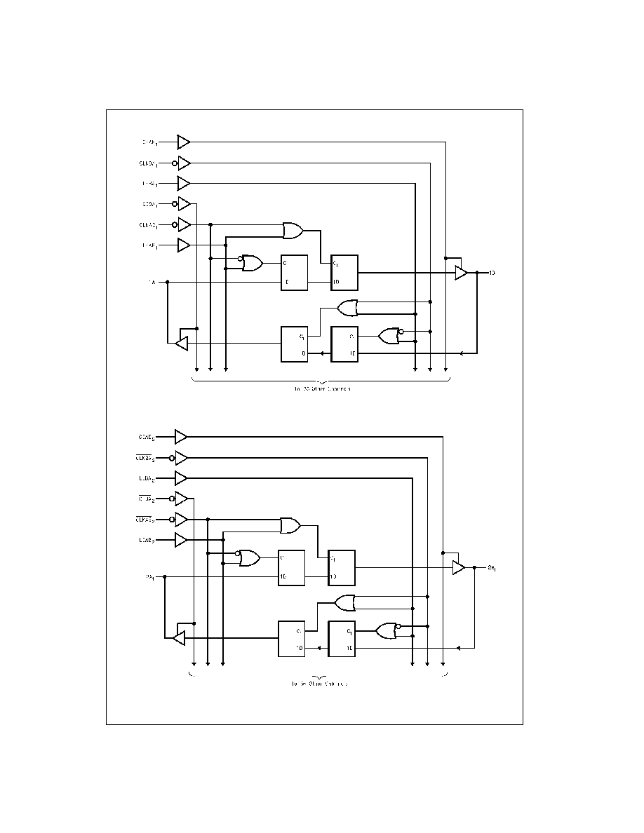
The VCX32500 is an 36-bit universal bus transceiver which
combines D-type latches and D-type flip-flops to allow data
flow in transparent, latched, and clocked modes.
Data flow in each direction is controlled by output-enable
(OEAB and OEBA), latch-enable (LEAB and LEBA), and
clock (CLKAB and CLKBA) inputs. For A-to-B data flow, the
device operates in the transparent mode when LEAB is
HIGH. When LEAB is LOW, the A data is latched if CLKAB
is held at a HIGH or LOW logic level. If LEAB is LOW, the A
bus data is stored in the latch/flip-flop on the HIGH-to-LOW
transition of CLKAB. When OEAB is HIGH, the outputs are
active. When OEAB is LOW, the outputs are in a high-
impedance state.
Data flow for B to A is similar to that of A to B but uses
OEBA, LEBA, and CLKBA. The output enables are com-
plementary (OEAB is active HIGH and OEBA is active
LOW).
The VCX32500 is designed for low voltage (1.4V to 3.6V)
V
CC
applications with I/O capability up to 3.6V.
The 74VCX32500 is fabricated with an advanced CMOS
technology to achieve high speed operation while maintain-
ing low CMOS power dissipation.
Features
s
1.4V to 3.6V V
CC
supply operation
s
3.6V tolerant inputs and outputs
s
t
PD
(A to B, B to A)
2.9 ns max for 3.0V to 3.6V V
CC
s
Power-down high impedance inputs and outputs
s
Supports live insertion/withdrawal (Note 1)
s
Static Drive (I
OH
/I
OL
)
±
24 mA @ 3.0V V
CC
s
Uses patented noise/EMI reduction circuitry
s
Latchup performance exceeds 300 mA
s
ESD performance:
Human body model
>
2000V
Machine model
>
200V
s
Packaged in plastic Fine-Pitch Ball Grid Array (FBGA)
Note 1: To ensure the high-impedance state during power up or power
down, OEBA should be tied to V
CC
through a pull-up resistor and OEAB
should be tied to GND through a pull-down resistors; the minimum value of
the resistor is determined by the current-sourcing capability of the driver.
Ordering Code:
Note 2: Ordering Code "G" indicates Trays.
Note 3: Devices also available in Tape and Reel. Specify by appending the suffix letter "X" to the ordering code.
Order Number
Package Number
Package Description
74VCX32500G
(Note 2)(Note 3)
BGA114A
114-Ball Fine-Pitch Ball Grid Array (FBGA), JEDEC MO-205, 5.5mm Wide
www.fairchildsemi.com
2
74VCX32500
Connection Diagram
(Top Thru View)
Pin Descriptions
FBGA Pin Assignments
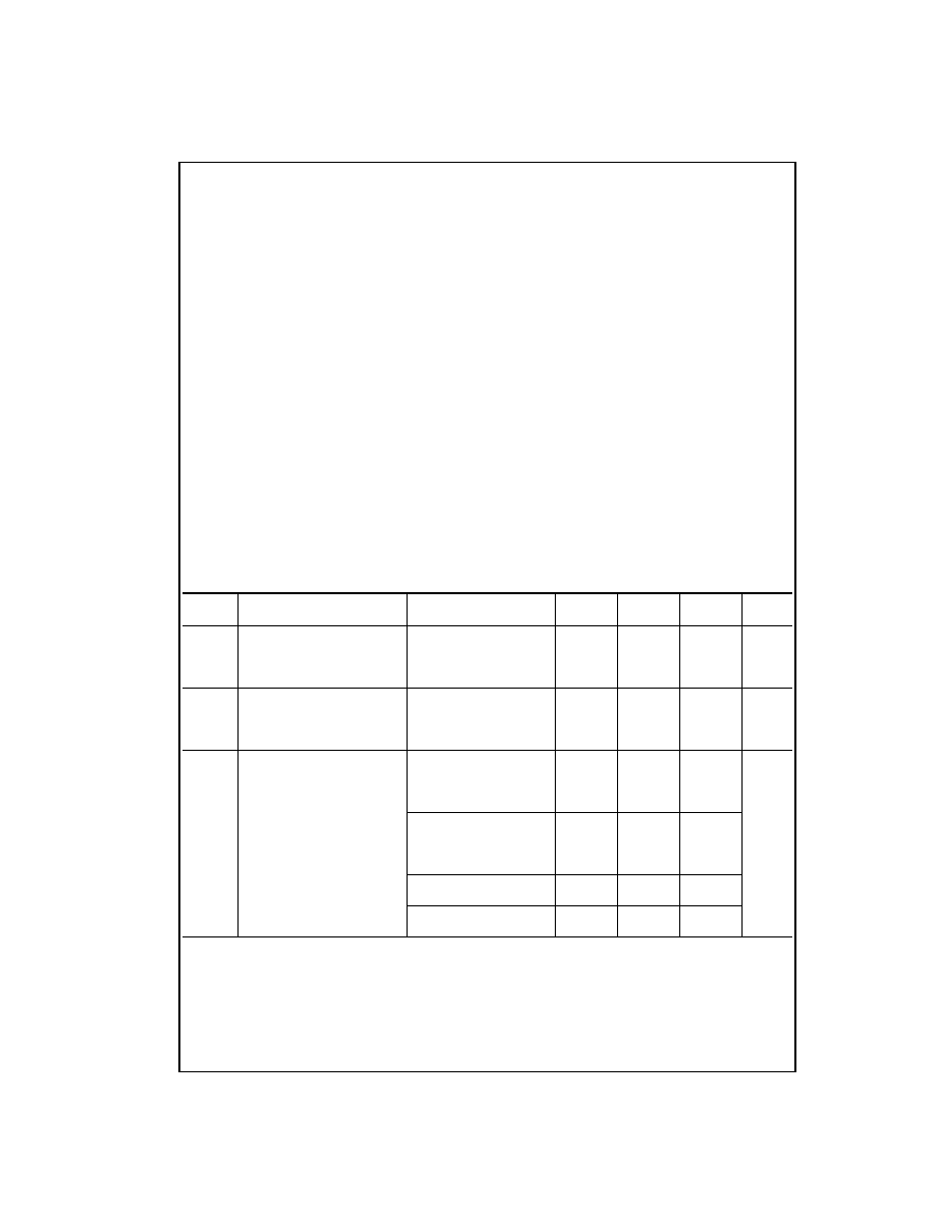
Function Table
(Note 4)
H
=
HIGH Voltage Level
L
=
LOW Voltage Level
X
=
Immaterial (HIGH or LOW, inputs may not float)
Z
=
High Impedance
Note 4: A-to-B data flow is shown; B-to-A flow is similar but uses OEBA,
LEBA and CLKBA. OEBA is active LOW.
Note 5: Output level before the indicated steady-state input conditions
were established.
Note 6: Output level before the indicated steady-state input conditions
were established, provided that CLKAB was LOW before LEAB went LOW.
Pin Names
Description
OEAB
n
Output Enable Input for A to B Direction
(Active HIGH)
OEBA
n
Output Enable Input for B to A Direction
(Active LOW)
LEAB
n
, LEBA
n
Latch Enable Inputs
CLKAB
n
,
CLKBA
n
Clock Inputs
1A
1
1A
18
2A
1
2A
18
Side A Inputs or 3-STATE Outputs
1B
1
1B
18
2B
1
2B
18
Side B Inputs or 3-STATE Outputs
1
2
3
4
5
6
A
1A
2
1A
1
LEAB
1
CLKAB
1
1B
1
1B
2
B
1A
4
1A
3
OEAB
1
GND
1B
3
1B
4
C
1A
6
1A
5
GND
GND
1B
5
1B
6
D
1A
8
1A
7
V
CC
V
CC
1B
7
1B
8
E
1A
10
1A
9
GND
GND
1B
9
1B
10
F
1A
12
1A
11
GND
GND
1B
11
1B
12
G
1A
14
1A
13
V
CC
V
CC
1B
13
1B
14
H
1A
15
1A
16
GND
GND
1B
16
1B
15
J
1A
17
1A
18
OEBA
1
CLKBA
1
1B
18
1B
17
K
NC
LEAB
2
LEBA
1
GND
CLKAB
2
NC
L
2A
2
2A
1
OEAB
2
GND
2B
1
2B
2
M
2A
4
2A
3
GND
GND
2B
3
2B
4
N
2A
6
2A
5
V
CC
V
CC
2B
5
2B
6
P
2A
8
2A
7
GND
GND
2B
7
2B
8
R
2A
10
2A
9
GND
GND
2B
9
2B
10
T
2A
12
2A
11
V
CC
V
CC
2B
11
2B
12
U
2A
14
2A
13
GND
GND
2B
13
2B
14
V
2A
15
2A
16
OEBA
2
CLKBA
2
2B
16
2B
15
W
2A
17
2A
18
LEBA
2
GND
2B
18
2B
17
Inputs
Outputs
OEAB
n
LEAB
n
CLKAB
n
A
n
B
n
L
X
X
X
Z
H
H
X
L
L
H
H
X
H
H
H
L
L
L
H
L
H
H
H
L
H
X
B
0
(Note 5)
H
L
L
X
B
0
(Note 6)
www.fairchildsemi.com
4
74VCX32500
Absolute Maximum Ratings
(Note 7)
Recommended Operating
Conditions
(Note 9)
Note 7: The "Absolute Maximum Ratings" are those values beyond which
the safety of the device cannot be guaranteed. The device should not be
operated at these limits. The parametric values defined in the Electrical
Characteristics tables are not guaranteed at the Absolute Maximum Rat-
ings. The Recommended Operating Conditions tables will define the condi-
tions for actual device operation.
Note 8: I
O
Absolute Maximum Rating must be observed.
Note 9: Floating or unused pin (inputs or I/O's) must be held HIGH or LOW.
DC Electrical Characteristics
Supply Voltage (V
CC
)
-
0.5V to
+
4.6V
DC Input Voltage (V
I
)
-
0.5V to
+
4.6V
Output Voltage (V
O
)
Outputs 3-STATE
-
0.5V to
+
4.6V
Outputs Active (Note 8)
-
0.5 to V
CC
+
0.5V
DC Input Diode Current (I
IK
) V
I
<
0V
-
50 mA
DC Output Diode Current (I
OK
)
V
O
<
0V
-
50 mA
V
O
>
V
CC
+
50 mA
DC Output Source/Sink Current
(I
OH
/I
OL
)
±
50 mA
DC V
CC
or Ground Current per
Supply Pin (I
CC
or GND)
±
100 mA
Storage Temperature Range (T
STG
)
-
65
°
C to
+
150
°
C
Power Supply
Operating
1.4V to 3.6V
Input Voltage
-
0.3V to 3.6V
Output Voltage (V
O
)
Output in Active States
0V to V
CC
Output in 3-STATE
0V to 3.6V
Output Current in I
OH
/I
OL
V
CC
=
3.0V to 3.6V
±
24 mA
V
CC
=
2.3V to 2.7V
±
18 mA
V
CC
=
1.65V to 2.3V
±
6 mA
V
CC
=
1.4V to 1.6V
±
2 mA
Free Air Operating Temperature (T
A
)
-
40
°
C to
+
85
°
C
Minimum Input Edge Rate (
t/
V)
V
IN
=
0.8V to 2.0V, V
CC
=
3.0V
10 ns/V
Symbol
Parameter
Conditions
V
CC
Min
Max
Units
(V)
V
IH
HIGH Level Input Voltage
2.7 - 3.6
2.0
V
2.3 - 2.7
1.6
1.65 - 2.3
0.65 x V
CC
1.4 - 1.6
0.65 x V
CC
V
IL
LOW Level Input Voltage
2.7 - 3.6
0.8
V
2.3 - 2.7
0.7
1.65 - 2.3
0.35 x V
CC
1.4 - 1.6
0.35 x V
CC
V
OH
HIGH Level Output Voltage
I
OH
=
-
100
µ
A
2.7 - 3.6
V
CC
-
0.2
V
I
OH
=
-
12 mA
2.7
2.2
I
OH
=
-
18 mA
3.0
2.4
I
OH
=
-
24 mA
3.0
2.2
I
OH
=
-
100
µ
A
2.3 - 2.7
V
CC
-
0.2
I
OH
=
-
6 mA
2.3
2.0
I
OH
=
-
12 mA
2.3
1.8
I
OH
=
-
18 mA
2.3
1.7
I
OH
=
-
100
µ
A
1.65 -2.3
V
CC
-
0.2
I
OH
=
-
6 mA
1.65
1.25
I
OH
=
-
100
µ
A
1.4 - 1.6
V
CC
-
0.2
I
OH
=
-
2 mA
1.4
1.05