© 2005 Fairchild Semiconductor Corporation
DS500163
www.fairchildsemi.com
July 1999
Revised February 2005
7
4
VC
X86
Low V
o
l
t
age Quad
2-
Inp
u
t Exclusi
ve-
O
R
Gate wit
h
3.
6V T
o
ler
ant Input
s
and Output
s
74VCX86
Low Voltage Quad 2-Input Exclusive-OR Gate with
3.6V Tolerant Inputs and Outputs
General Description
The VCX86 contains four 2-input exclusive OR gates. This
product is designed for low voltage (1.2V to 3.6V) V
CC
applications with I/O compatibility up to 3.6V
The 74VCX86 is fabricated with an advanced CMOS tech-
nology to achieve high-speed operation while maintaining
low CMOS power dissipation.
Features
s
1.2V to 3.6V V
CC
supply operation
s
3.6V tolerant inputs and outputs
s
t
PD
3.0 ns max for 3.0V to 3.6V V
CC
s
Power-off high impedance inputs and outputs
s
Static Drive (I
OH
/I
OL
)
r
24 mA @ 3.0V V
CC
s
Uses patented noise/EMI reduction circuitry
s
Latchup performance exceeds JEDEC 78 conditions
s
ESD performance:
Human body model
!
2000V
Machine model
!
250V
s
Leadless Pb-Free DQFN package
Ordering Code:
Devices also available in Tape and Reel. Specify by appending the suffix letter "X" to the ordering code.
Pb-Free package per JEDEC J-STD-020B.
Note 1: DQFN package available in Tape and Reel only.
Order Number Package Number
Package Description
74VCX86M
M14A
14-Lead Small Outline Integrated Circuit (SOIC), JEDEC MS-012, 0.150" Narrow
74VCX86BQX
(Note 1)
MLP014A
Pb-Free 14-Terminal Depopulated Quad Very-Thin Flat Pack No Leads (DQFN), JEDEC
MO-241, 2.5 x 3.0mm
74VCX86MTC
MTC14
14-Lead Thin Shrink Small Outline Package (TSSOP), JEDEC MO-153, 4.4mm Wide
www.fairchildsemi.com
2
7
4
VC
X86
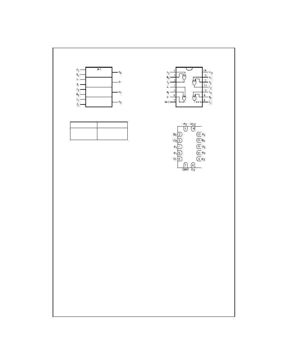
Logic Symbol
IEEE/IEC
Pin Descriptions
Connection Diagrams
Pin Assignments for SOIC and TSSOP
Pad Assignments for DQFN
(Top View)
Pin Names
Description
A
n
, B
n
Inputs
O
n
Outputs
3
www.fairchildsemi.com
7
4
VC
X86
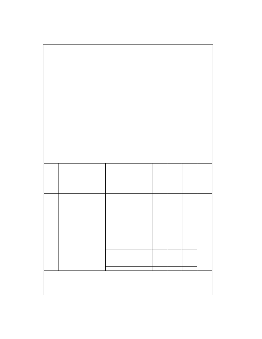
Absolute Maximum Ratings
(Note 2)
Recommended Operating
Conditions
(Note 4)
Note 2: The Absolute Maximum Ratings are those values beyond which
the safety of the device cannot be guaranteed. The device should not be
operated at these limits. The parametric values defined in the Electrical
Characteristics tables are not guaranteed at the Absolute Maximum Rat-
ings. The "Recommended Operating Conditions" table will define the condi-
tions for actual device operation.
Note 3: I
O
Absolute Maximum Rating must be observed.
Note 4: Floating or unused inputs must be held HIGH or LOW.
DC Electrical Characteristics
Supply Voltage (V
CC
)
0.5V to
4.6V
DC Input Voltage (V
I
)
0.5V to
4.6V
Output Voltage (V
O
)
HIGH or LOW State (Note 3)
0.5V to V
CC
0.5V
V
CC
0V
0.5V to
4.6V
DC Input Diode Current (I
IK
) V
I
0V
50 mA
DC Output Diode Current (I
OK
)
V
O
0V
50 mA
V
O
!
V
CC
50 mA
DC Output Source/Sink Current
(I
OH
/I
OL
)
r
50 mA
DC V
CC
or GND Current per
Supply Pin (I
CC
or Ground)
r
100 mA
Storage Temperature Range (T
STG
)
65
q
C to
150
q
C
Power Supply
Operating
1.2V to 3.6V
Input Voltage
0.3V to
3.6V
Output Voltage (V
O
)
HIGH or LOW State
0V to V
CC
Output Current in I
OH
/I
OL
V
CC
3.0V to 3.6V
r
24 mA
V
CC
2.3V to 2.7V
r
18 mA
V
CC
1.65V to 2.3V
r
6 mA
V
CC
1.4V to 1.6V
r
2 mA
V
CC
1.2V
r
100
P
A
Free Air Operating Temperature (T
A
)
40
q
C to
85
q
C
Minimum Input Edge Rate (
'
t/
'
V)
V
IN
0.8V to 2.0V, V
CC
3.0V
10 ns/V
Symbol
Parameter
Conditions
V
CC
Min
Max
Units
(V)
V
IH
HIGH Level Input Voltage
2.7 - 3.6
2.0
V
2.3 - 2.7
1.6
1.65 - 2.3
0.65
u
V
CC
1.4 - 1.6
0.65
u
V
CC
1.2
0.65
u
V
CC
V
IL
LOW Level Input Voltage
2.7 - 3.6
0.8
V
2.3 - 2.7
0.7
1.65 - 2.3
0.35
u
V
CC
1.4 - 1.6
0.35
u
V
CC
1.2
V
OH
HIGH Level Output Voltage
I
OH
100
P
A
2.7 - 3.6
V
CC
- 0.2
V
I
OH
12 mA
2.7
2.2
I
OH
18 mA
3.0
2.4
I
OH
24 mA
3.0
2.2
I
OH
100
P
A
2.3 - 2.7
V
CC
- 0.2
I
OH
6 mA
2.3
2.0
I
OH
12 mA
2.3
1.8
I
OH
18 mA
2.3
1.7
I
OH
100
P
A
1.65 - 2.3
V
CC
- 0.2
I
OH
6 mA
1.65
1.25
I
OH
100
P
A
1.4 - 1.6
V
CC
- 0.2
I
OH
2 mA
1.4
1.05
I
OH
100
P
A
1.2
V
CC
- 0.2
www.fairchildsemi.com
4
7
4
VC
X86
DC Electrical Characteristics
(Continued)
AC Electrical Characteristics
(Note 5)
Note 5: For C
L
50
P
F, add approximately 300 ps to the AC maximum specification.
Note 6: Skew is defined as the absolute value of the difference between the actual propagation delay for any two separate outputs of the same device. The
specification applies to any outputs switching in the same direction, either HIGH-to-LOW (t
OSHL
) or LOW-to-HIGH (t
OSLH
).
Symbol
Parameter
Conditions
V
CC
Min
Max
Units
(V)
V
OL
LOW Level Output Voltage
I
OL
100
P
A
2.7 - 3.6
0.2
V
I
OL
12 mA
2.7
0.4
I
OL
18 mA
3.0
0.4
I
OL
24 mA
3.0
0.55
I
OL
100
P
A
2.3 - 2.7
0.2
I
OL
12 mA
2.3
0.4
I
OL
18 mA
2.3
0.6
I
OL
100
P
A
1.65 - 2.3
0.2
I
OL
6 mA
1.65
0.3
I
OL
100
P
A
1.4 - 1.6
0.2
I
OL
2 mA
1.4
0.35
I
OL
100
P
A
1.2
0.05
I
I
Input Leakage Current
0
d
V
I
d
3.6V
1.2 - 3.6
r
5.0
P
A
I
OFF
Power-OFF Leakage Current
0
d
(V
I
, V
O
)
d
3.6V
0
10
P
A
I
CC
Quiescent Supply Current
V
I
V
CC
or GND
1.2 - 3.6
20
P
A
V
CC
d
(V
I
) 1.2
-
3.6
r
20
'
I
CC
Increase in I
CC
per Input
V
IH
V
CC
0.6V
2.7 - 3.6
750
P
A
Symbol
Parameter
Conditions
V
CC
T
A
40
q
C to
85
q
C
Units
Figure
(V)
Min
Max
Number
t
PHL
Propagation Delay
C
L
30 pF, R
L
500
:
3.3
r
0.3
0.6
3.0
ns
Figures
1, 2
t
PLH
2.5
r
0.2
0.8
3.9
1.8
r
0.15
1.0
7.8
C
L
15 pF, R
L
2k
:
1.5
r
0.1
1.0
15.6
Figures
3, 4
1.2
1.5
39
t
OSHL
Output to Output Skew
C
L
30 pF, R
L
500
:
3.3
r
0.3
0.5
ns
t
OSLH
(Note 6)
2.5
r
0.2
0.5
1.8
r
0.15
0.75
C
L
15 pF, R
L
2k
:
1.5
r
0.1
1.5
1.2
1.5
5
www.fairchildsemi.com
7
4
VC
X86
Dynamic Switching Characteristics
Capacitance
AC Loading and Waveforms (V
CC
3.3V
r
0.3V to 1.8V
r
0.15V)
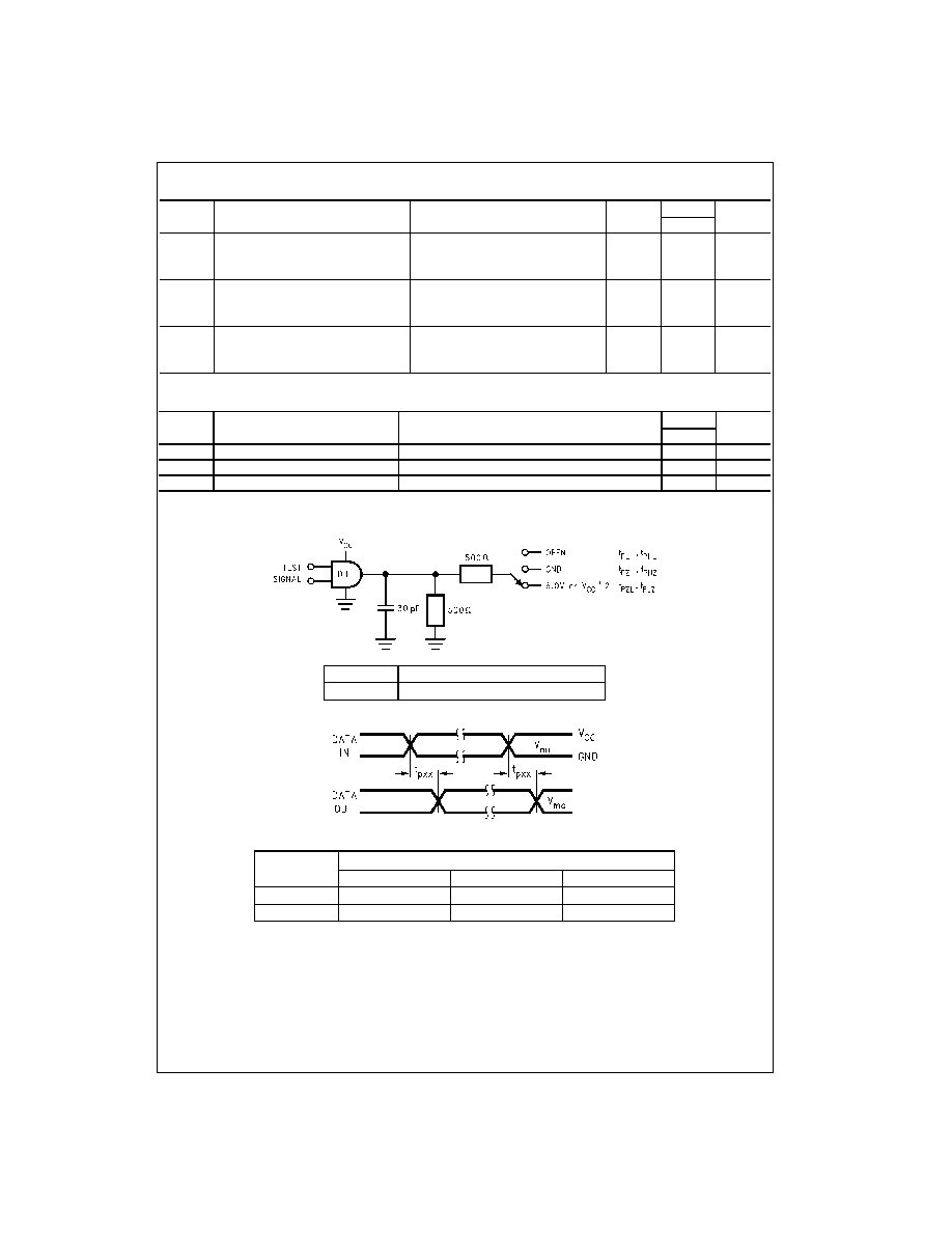
FIGURE 1. AC Test Circuit
FIGURE 2. Waveform for Inverting and Non-Inverting Functions
Symbol
Parameter
Conditions
V
CC
T
A
25
q
C
Units
(V)
Typical
V
OLP
Quiet Output Dynamic Peak V
OL
C
L
30 pF, V
IH
V
CC
, V
IL
0V
1.8
0.25
V
2.5
0.6
3.3
0.8
V
OLV
Quiet Output Dynamic Valley V
OL
C
L
30 pF, V
IH
V
CC
, V
IL
0V
1.8
0.25
V
2.5
0.6
3.3
0.8
V
OHV
Quiet Output Dynamic Valley V
OH
C
L
30 pF, V
IH
V
CC
, V
IL
0V
1.8
1.5
V
2.5
1.9
3.3
2.2
Symbol
Parameter
Conditions
T
A
25
q
C
Units
Typical
C
IN
Input Capacitance
V
CC
1.8, 2.5V or 3.3V, V
I
0V or V
CC
6
pF
C
OUT
Output Capacitance
V
I
0V or V
CC
, V
CC
1.8V, 2.5V or 3.3V
7
pF
C
PD
Power Dissipation Capacitance
V
I
0V or V
CC
, f
10 MHz, V
CC
1.8V, 2.5V or 3.3V
20
pF
TEST
SWITCH
t
PLH
, t
PHL
Open
Symbol
V
CC
3.3V
r
0.3V
2.5V
r
0.2V
1.8V
r
0.15V
V
mi
1.5V
V
CC
/2
V
CC
/2
V
mo
1.5V
V
CC
/2
V
CC
/2
www.fairchildsemi.com
6
7
4
VC
X86
AC Loading and Waveforms (V
CC
1.5V
r
0.1V to 1.2V)
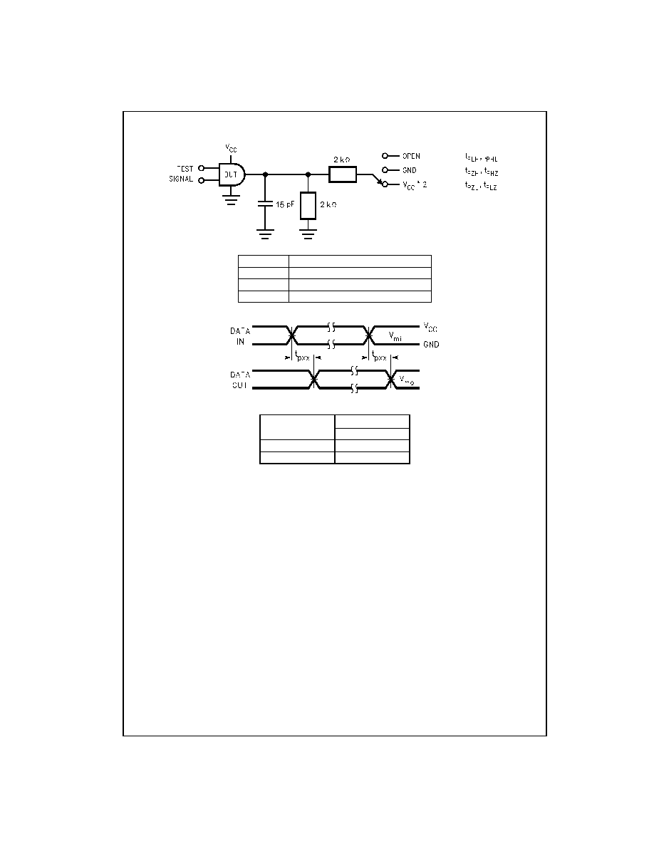
FIGURE 3. AC Test Circuit
FIGURE 4. Waveform for Inverting and Non-Inverting Functions
TEST
SWITCH
t
PLH
, t
PHL
Open
t
PZL
, t
PLZ
V
CC
x 2 at V
CC
1.5
r
0.1V
t
PZH
, t
PHZ
GND
Symbol
V
CC
1.5V
r
0.1V
V
mi
V
CC
/2
V
mo
V
CC
/2
7
www.fairchildsemi.com
7
4
VC
X86
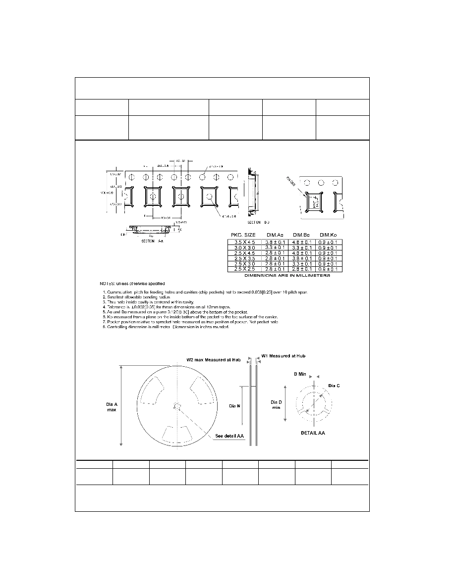
Tape and Reel Specification
Tape Format for DQFN
TAPE DIMENSIONS inches (millimeters)
REEL DIMENSIONS inches (millimeters)
Package
Tape
Number
Cavity
Cover Tape
Designator
Section
Cavities
Status
Status
Leader (Start End)
125 (typ)
Empty
Sealed
BQX
Carrier
2500/3000
Filled
Sealed
Trailer (Hub End)
75 (typ)
Empty
Sealed
Tape Size
A
B
C
D
N
W1
W2
12 mm
13.0
0.059
0.512
0.795
7.008
0.488
0.724
(330)
(1.50)
(13.00)
(20.20)
(178)
(12.4)
(18.4)
www.fairchildsemi.com
8
7
4
VC
X86
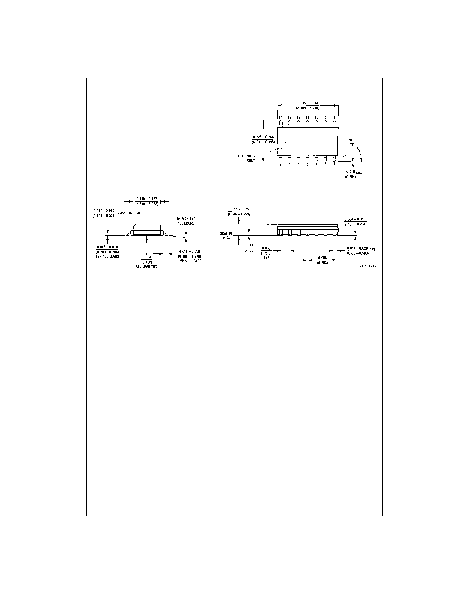
Physical Dimensions
inches (millimeters) unless otherwise noted
14-Lead Small Outline Integrated Circuit (SOIC), JEDEC MS-012, 0.150" Narrow
Package Number M14A
9
www.fairchildsemi.com
7
4
VC
X86
Physical Dimensions
inches (millimeters) unless otherwise noted (Continued)
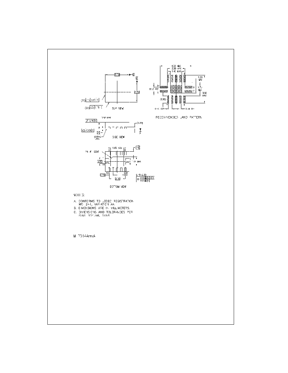
Pb-Free 14-Terminal Depopulated Quad Very-Thin Flat Pack No Leads (DQFN), JEDEC MO-241, 2.5 x 3.0mm
Package Number MLP014A
www.fairchildsemi.com
10
7
4
VC
X86
Low V
o
l
t
age Quad
2-
Inp
u
t Exclusi
ve-
O
R
Gate wit
h
3.
6V T
o
l
e
r
ant Input
s
and Output
s
Physical Dimensions
inches (millimeters) unless otherwise noted (Continued)
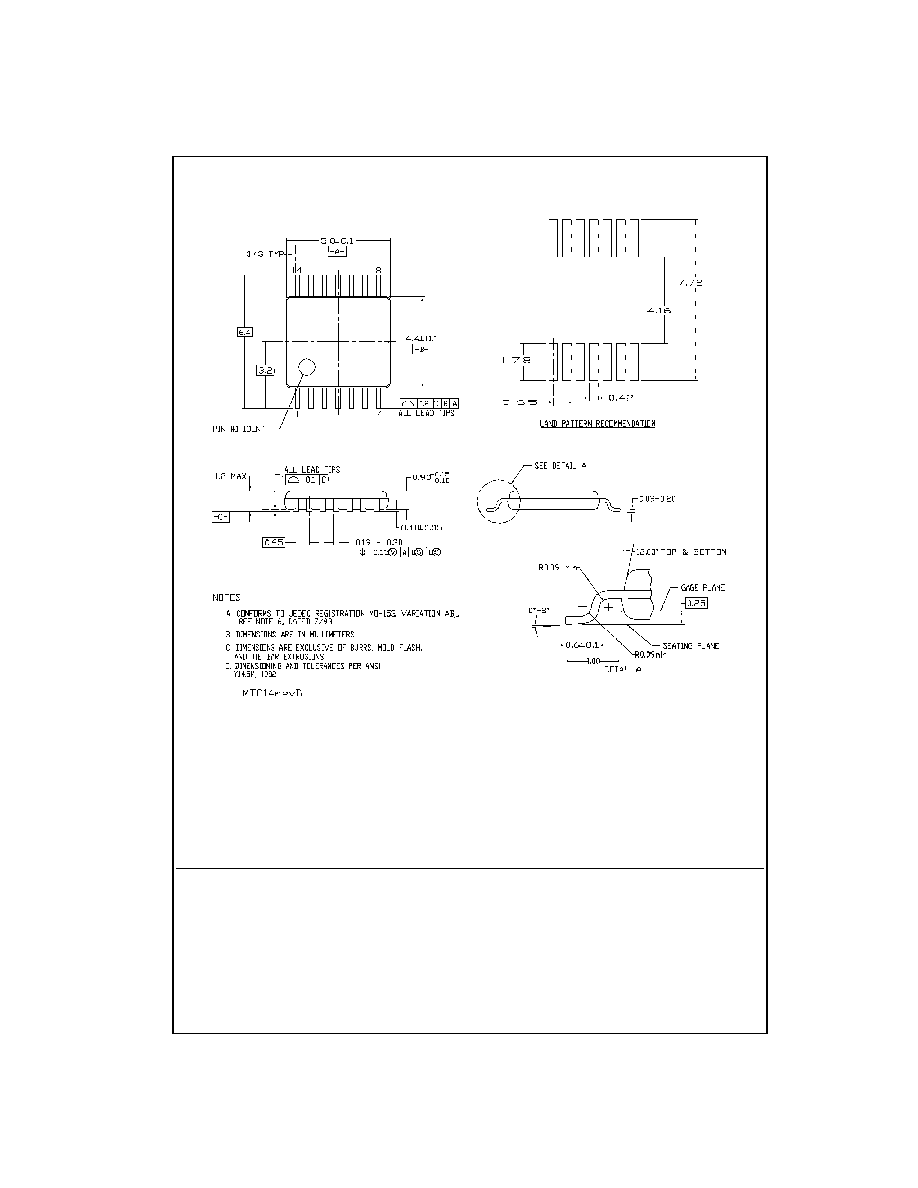
14-Lead Thin Shrink Small Outline Package (TSSOP), JEDEC MO-153, 4.4mm Wide
Package Number MTC14
Fairchild does not assume any responsibility for use of any circuitry described, no circuit patent licenses are implied and
Fairchild reserves the right at any time without notice to change said circuitry and specifications.
LIFE SUPPORT POLICY
FAIRCHILD'S PRODUCTS ARE NOT AUTHORIZED FOR USE AS CRITICAL COMPONENTS IN LIFE SUPPORT
DEVICES OR SYSTEMS WITHOUT THE EXPRESS WRITTEN APPROVAL OF THE PRESIDENT OF FAIRCHILD
SEMICONDUCTOR CORPORATION. As used herein:
1. Life support devices or systems are devices or systems
which, (a) are intended for surgical implant into the
body, or (b) support or sustain life, and (c) whose failure
to perform when properly used in accordance with
instructions for use provided in the labeling, can be rea-
sonably expected to result in a significant injury to the
user.
2. A critical component in any component of a life support
device or system whose failure to perform can be rea-
sonably expected to cause the failure of the life support
device or system, or to affect its safety or effectiveness.
www.fairchildsemi.com