© 2000 Fairchild Semiconductor Corporation
DS500231
www.fairchildsemi.com
January 2000
Revised March 2000
7
4
VC
XH162
244
Lo
w
V
o
lt
age
1
6
-Bi
t
Buff
er/
L
ine Dri
ver wit
h
Busho
ld
74VCXH162244
Low Voltage 16-Bit Buffer/Line Driver with Bushold
and 26
Series Resistor in Outputs
General Description
The VCXH162244 contains sixteen non-inverting buffers
with 3-STATE outputs to be employed as a memory and
address driver, clock driver, or bus oriented transmitter/
receiver. The device is nibble (4-bit) controlled. Each nibble
has separate 3-STATE control inputs which can be shorted
together for full 16-bit operation. .
The VCXH162244 data inputs include active bushold cir-
cuitry, eliminating the need for external pull-up resistors to
hold unused or floating data inputs at a valid logic level
The 74VCXH162244 is also designed with 26
series
resistors in the outputs. This design reduces line noise in
applications such as memory address drivers, clock driv-
ers, and bus transceivers/transmitters.
The 74VCXH162244 is designed for low voltage (1.65V to
3.6V) V
CC
applications with output capability up to 3.6V.
The 74VCXH162244 is fabricated with an advanced CMOS
technology to achieve high speed operation while maintain-
ing low CMOS power dissipation.
Features
s
1.65V≠3.6V V
CC
supply operation
s
3.6V tolerant control inputs and outputs
s
Bushold on data inputs eliminates the need for external
pull-up/pull-down resistors
s
26
series resistors in outputs
s
t
PD
3.3 ns max for 3.0V to 3.6V V
CC
3.8 ns max for 2.3V to 2.7V V
CC
7.6 ns max for 1.65V to 1.95V V
CC
s
Static Drive (I
OH
/I
OL
)
±
12 mA @ 3.0V V
CC
±
8 mA @ 2.3V V
CC
±
3
mA @
1.65V
V
CC
s
Uses patented noise/EMI reduction circuitry
s
Latch-up performance exceeds 300 mA
s
ESD performance:
Human body model
>
2000V
Machine model
>
200V
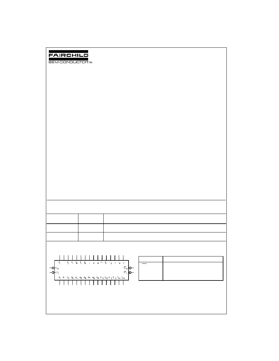
Ordering Code:
Note 1: Use this Order Number to receive devices in Tape and Reel.
Logic Symbol
Pin Descriptions
Order Number
Package
Package Description
Number
74VCXH162244MTD
MTD48
48-Lead Thin Shrink Small Outline Package (TSSOP), JEDEC MO-153, 6.1mm Wide
[TUBES]
74VCXH162244MTX
(Note 1)
MTD48
48-Lead Thin Shrink Small Outline Package (TSSOP), JEDEC MO-153, 6.1mm Wide
[TAPE and REEL]
Pin Names
Description
OE
n
Output Enable Input (Active LOW)
I
0
≠I
15
Bushold Inputs
O
0
≠O
15
Outputs
www.fairchildsemi.com
2
74VCXH162244
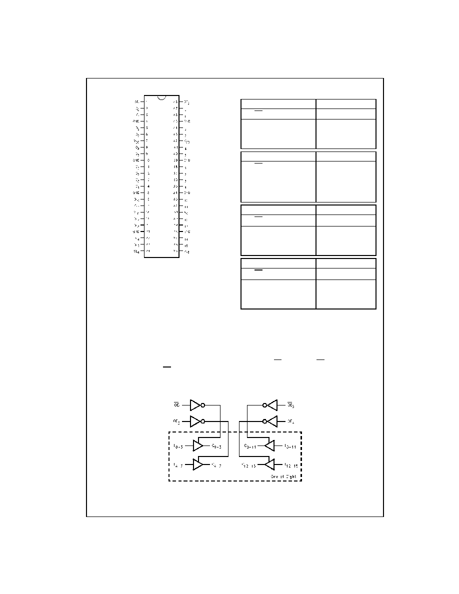
Connection Diagram
Truth Tables
H
=
HIGH Voltage Level
L
=
LOW Voltage Level
X
=
Immaterial (HIGH or LOW, inputs may not float)
Z
=
High Impedance
Functional Description
The 74VCXH162244 contains sixteen non-inverting buffers with 3-STATE outputs. The device is nibble (4 bits) controlled
with each nibble functioning identically, but independent of each other. The control pins may be shorted together to obtain
full 16-bit operation.The 3-STATE outputs are controlled by an Output Enable (OE
n
) input. When OE
n
is LOW, the outputs
are in the 2-state mode. When OE
n
is HIGH, the standard outputs are in the high impedance mode but this does not inter-
fere with entering new data into the inputs.
Logic Diagram
Inputs
Outputs
OE
1
I
0
≠I
3
O
0
≠O
3
L
L
L
L
H
H
H
X
Z
Inputs
Outputs
OE
2
I
4
≠I
7
O
4
≠O
7
L
L
L
L
H
H
H
X
Z
Inputs
Outputs
OE
3
I
8
≠I
11
O
8
≠O
11
L
L
L
L
H
H
H
X
Z
Inputs
Outputs
OE
4
I
12
≠I
15
O
12
≠O
15
L
L
L
L
H
H
H
X
Z
3
www.fairchildsemi.com
7
4
VC
XH162
244
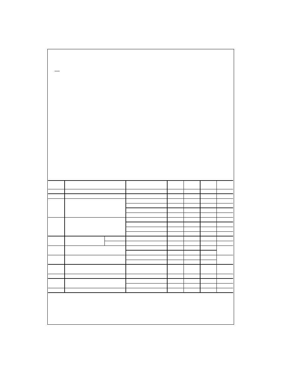
Absolute Maximum Ratings
(Note 2)
Recommended Operating
Conditions
(Note 4)
Note 2: The Absolute Maximum Ratings are those values beyond which
the safety of the device cannot be guaranteed. The device should not be
operated at these limits. The parametric values defined in the Electrical
Characteristics tables are not guaranteed at the Absolute Maximum Rat-
ings. The "Recommended Operating Conditions" table will define the condi-
tions for actual device operation.
Note 3: I
O
Absolute Maximum Rating must be observed.
Note 4: Floating or unused control inputs must be held HIGH or LOW.
DC Electrical Characteristics (2.7V
<
V
CC
3.6V)
Note 5: An external driver must source at least the specified current to switch from LOW-to-HIGH.
Note 6: An external driver must sink at least the specified current to switch from HIGH-to-LOW.
Note 7: Outputs disabled or 3-STATE only.
Supply Voltage (V
CC
)
-
0.5V to
+
4.6V
DC Input Voltage (V
I
)
OE
n
-
0.5V to 4.6V
I
0
≠ I
15
-
0.5V to V
CC
+
0.5V
Output Voltage (V
O
)
Outputs 3-STATE
-
0.5V to
+
4.6V
Outputs Active (Note 3)
-
0.5V to V
CC
+
0.5V
DC Input Diode Current (I
IK
)
V
I
<
0V
-
50 mA
DC Output Diode Current (I
OK
)
V
O
<
0V
-
50 mA
V
O
>
V
CC
+
50 mA
DC Output Source/Sink Current
(I
OH
/I
OL
)
±
50 mA
DC V
CC
or GND Current per
Supply Pin (I
CC
or GND)
±
100 mA
Storage Temperature Range (T
STG
)
-
65
∞
C to
+
150
∞
C
Power Supply
Operating
1.65V to 3.6V
Data Retention Only
1.2V to 3.6V
Input Voltage
-
0.3V to V
CC
Output Voltage (V
O
)
Output in Active States
0V to V
CC
Output in 3-STATE
0.0V to 3.6V
Output Current in I
OH
/I
OL
V
CC
=
3.0V to 3.6V
±
12 mA
V
CC
=
2.3V to 2.7V
±
8 mA
V
CC
=
1.65V to 2.3V
±
3mA
Free Air Operating Temperature (T
A
)
-
40
∞
C to
+
85
∞
C
Minimum Input Edge Rate (
t/
V)
V
IN
=
0.8V to 2.0V, V
CC
=
3.0V
10 ns/V
Symbol
Parameter
Conditions
V
CC
(V)
Min
Max
Units
V
IH
HIGH Level Input Voltage
2.7≠3.6
2.0
V
V
IL
LOW Level Input Voltage
2.7≠3.6
0.8
V
V
OH
HIGH Level Output Voltage
I
OH
=
-
100
µ
A 2.7≠3.6
V
CC
-
0.2
V
I
OH
=
-
6 mA
2.7
2.2
V
I
OH
=
-
8 mA
3.0
2.4
V
I
OH
=
-
12 mA
3.0
2.2
V
V
OL
LOW Level Output Voltage
I
OL
=
100
µ
A 2.7≠3.6
0.2
V
I
OL
=
6 mA
2.7
0.4
V
I
OL
=
8 mA
3.0
0.55
V
I
OL
=
12 mA
3.0
0.8
V
I
I
Input Leakage Current
Control Pins
0
V
I
3.6V
2.7≠3.6
±
5.0
µ
A
Data Pins
V
I
=
V
CC
or GND
2.7≠3.6
±
5.0
µ
A
I
I(HOLD)
Bushold Input Minimum
V
IN
=
0.8V
3.0
75
µ
A
Drive Hold Current
V
IN
=
2.0V
3.0
-
75
I
I(OD)
Bushold Input Over-Drive
(Note 5)
3.6
450
µ
A
Current to Change State
(Note 6)
3.6
-
450
I
OZ
3-STATE Output Leakage
0
V
O
3.6V
2.7≠3.6
±
10
µ
A
V
I
=
V
IH
or V
IL
I
OFF
Power-OFF Leakage Current
0
(V
O
)
3.6V
0
10
µ
A
I
CC
Quiescent Supply Current
V
I
=
V
CC
or GND
2.7≠3.6
20
µ
A
V
CC
(V
O
)
3.6V (Note 7)
2.7≠3.6
±
20
µ
A
I
CC
Increase in I
CC
per Input
V
IH
=
V
CC
-
0.6V
2.7≠3.6
750
µ
A
www.fairchildsemi.com
4
74VCXH162244
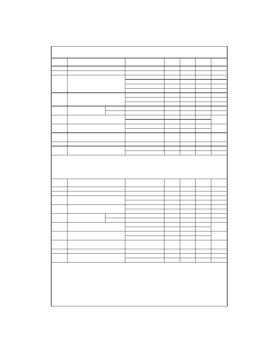
DC Electrical Characteristics (2.3V
V
CC
2.7V)
Note 8: An external driver must source at least the specified current to switch from LOW-to-HIGH.
Note 9: An external driver must sink at least the specified current to switch from HIGH-to-LOW.
Note 10: Outputs disabled or 3-STATE only.
DC Electrical Characteristics (1.65V
V
CC
<
2.3V)
Note 11: An external driver must source at least the specified current to switch from LOW-to-HIGH.
Note 12: An external driver must sink at least the specified current to switch from HIGH-to-LOW.
Note 13: Outputs disabled or 3-STATE only.
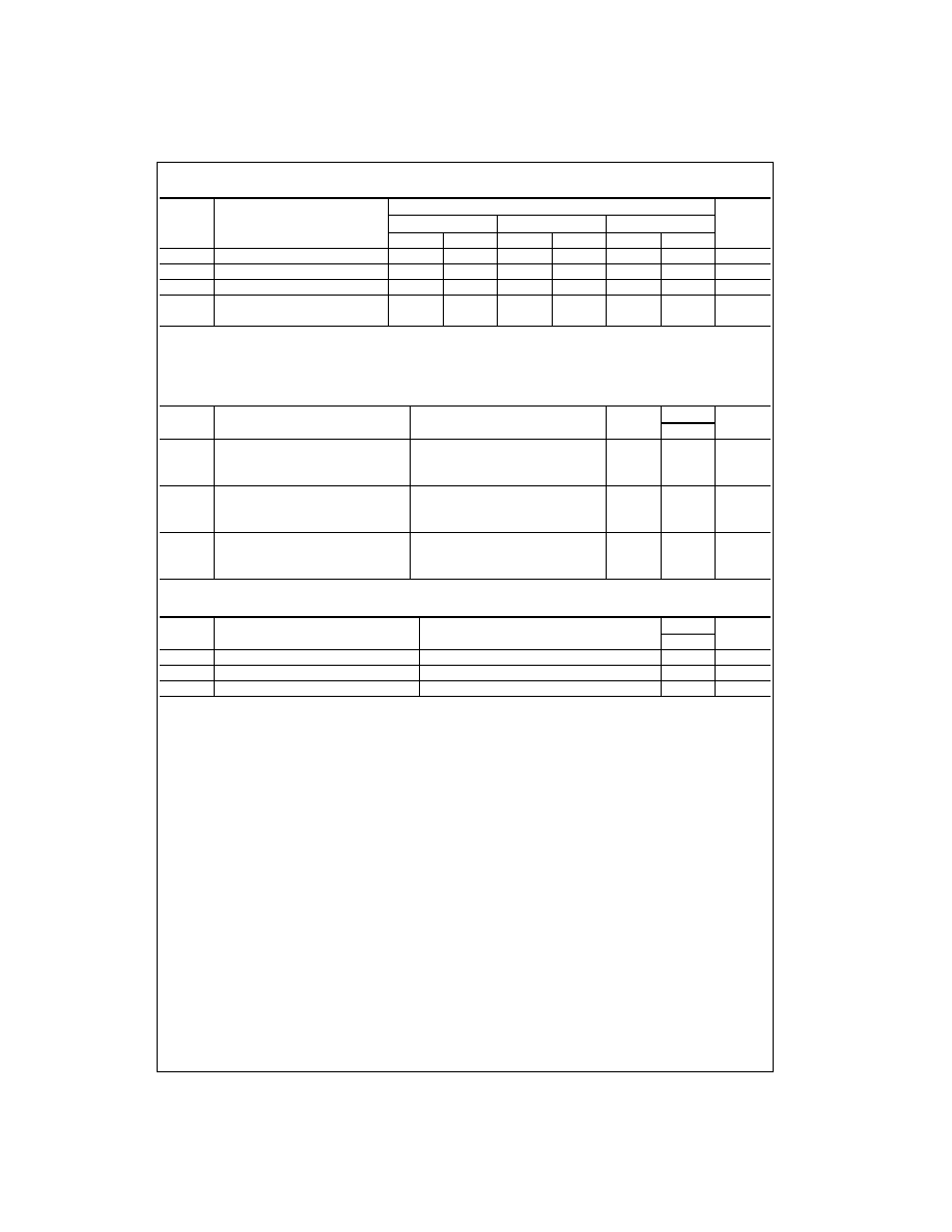
Symbol
Parameter
Conditions
V
CC
(V)
Min
Max
Units
V
IH
HIGH Level Input Voltage
2.3≠2.7
1.6
V
V
IL
LOW Level Input Voltage
2.3≠2.7
0.7
V
V
OH
HIGH Level Output Voltage
I
OH
=
-
100
µ
A 2.3≠2.7
V
CC
-
0.2
V
I
OH
=
-
4 mA
2.3
2.0
V
I
OH
=
-
6 mA
2.3
1.8
V
I
OH
=
-
8 mA
2.3
1.7
V
V
OL
LOW Level Output Voltage
I
OL
=
100
µ
A 2.3≠2.7
0.2
V
I
OL
=
6 mA
2.3
0.4
V
I
OL
=
8 mA
2.3
0.6
V
I
I
Input Leakage Current
Control Pins
0
V
I
3.6V
2.3≠2.7
±
5.0
µ
A
Data Pins
V
I
=
V
CC
or GND
2.3≠2.7
±
5.0
µ
A
I
I(HOLD)
Bushold Input Minimum
V
IN
=
0.7V
2.3
45
µ
A
Drive Hold Current
V
IN
=
1.6V
2.3
-
45
I
I(OD)
Bushold Input Over-Drive
(Note 8)
2.7
300
µ
A
Current to Change State
(Note 9)
2.7
-
300
I
OZ
3-STATE Output Leakage
0
V
O
3.6V
2.3≠2.7
±
10
µ
A
V
I
=
V
IH
or V
IL
I
OFF
Power-OFF Leakage Current
0
(V
O
)
3.6V
0
10
µ
A
I
CC
Quiescent Supply Current
V
I
=
V
CC
or GND
2.3≠2.7
20
µ
A
V
CC
(V
O
)
3.6V (Note 10)
2.3≠2.7
±
20
µ
A
Symbol
Parameter
Conditions
V
CC
(V)
Min
Max
Units
V
IH
HIGH Level Input Voltage
1.65-2.3
0.65
◊
V
CC
V
V
IL
LOW Level Input Voltage
1.65-2.3
0.35
◊
V
CC
V
V
OH
HIGH Level Output Voltage
I
OH
=
-
100
µ
A 1.65-2.3
V
CC
-
0.2
V
I
OH
=
-
3 mA
1.65
1.25
V
V
OL
LOW Level Output Voltage
I
OL
=
100
µ
A 1.65-2.3
0.2
V
I
OL
=
3mA
1.65
0.3
V
I
I
Input Leakage Current
Control Pins
0
V
I
3.6V
1.65-2.3
±
5.0
µ
A
Data Pins
V
I
=
V
CC
or GND
1.65-2.3
±
5.0
µ
A
I
I(HOLD)
Bushold Input Minimum
V
IN
=
0.57V
1.65
25
µ
A
Drive Hold Current
V
IN
=
1.07V
1.65
-
25
I
I(OD)
Bushold Input Over-Drive
(Note 11)
1.95
200
µ
A
Current to Change State
(Note 12)
1.95
-
200
I
OZ
3-STATE Output Leakage
0
V
O
3.6V
1.65-2.3
±
10
µ
A
V
I
=
V
IH
or V
IL
I
OFF
Power-OFF Leakage Current
0
(V
O
)
3.6V
0
10
µ
A
I
CC
Quiescent Supply Current
V
I
=
V
CC
or GND
1.65-2.3
20
µ
A
V
CC
(V
O
)
3.6V (Note 13)
1.65-2.3
±
20
µ
A
5
www.fairchildsemi.com
7
4
VC
XH162
244
AC Electrical Characteristics
(Note 14)
Note 14: For C
L
=
50
P
F, add approximately 300 ps to the AC maximum specification.
Note 15: Skew is defined as the absolute value of the difference between the actual propagation delay for any two separate outputs of the same device. The
specification applies to any outputs switching in the same direction, either HIGH-to-LOW (t
OSHL
) or LOW-to-HIGH (t
OSLH
).
Dynamic Switching Characteristics
Capacitance
Symbol
Parameter
T
A
=
-
40
∞
C to
+
85
∞
C, C
L
=
30 pF, R
L
=
500
Units
V
CC
=
3.3V
±
0.3V
V
CC
=
2.5V
±
0.2V
V
CC
=
1.8V
±
0.15V
Min
Max
Min
Max
Min
Max
t
PHL
, t
PLH
Prop Delay
0.8
3.3
1.0
3.8
1.5
7.6
ns
t
PZL
, t
PZH
Output Enable Time
0.8
3.8
1.0
5.1
1.5
9.8
ns
t
PLZ
, t
PHZ
Output Disable Time
0.8
3.6
1.0
4.0
1.5
7.2
ns
t
OSHL
Output to Output Skew
0.5
0.5
0.75
ns
t
OSLH
(Note 15)
Symbol
Parameter
Conditions
V
CC
T
A
=
+
25
∞
C
Units
(V)
Typical
V
OLP
Quiet Output Dynamic Peak V
OL
C
L
=
30 pF, V
IH
=
V
CC
, V
IL
=
0V
1.8
0.15
V
2.5
0.25
3.3
0.35
V
OLV
Quiet Output Dynamic Valley V
OL
C
L
=
30 pF, V
IH
=
V
CC
, V
IL
=
0V
1.8
-
0.15
V
2.5
-
0.25
3.3
-
0.35
V
OHV
Quiet Output Dynamic Valley V
OH
C
L
=
30 pF, V
IH
=
V
CC
, V
IL
=
0V
1.8
1.55
V
2.5
2.05
3.3
2.65
Symbol
Parameter
Conditions
T
A
=
+
25
∞
C
Units
Typical
C
IN
Input Capacitance
V
CC
=
1.8, 2.5V or 3.3V, V
I
=
0V or V
CC
6
pF
C
OUT
Output Capacitance
V
I
=
0V or V
CC
, V
CC
=
1.8V, 2.5V or 3.3V
7
pF
C
PD
Power Dissipation Capacitance
V
I
=
0V or V
CC
, f
=
10 MHz, V
CC
=
1.8V, 2.5V or 3.3V
20
pF