© 2000 Fairchild Semiconductor Corporation
DS500228
www.fairchildsemi.com
January 2000
Revised March 2000
7
4
VC
XH163
74
Low V
o
l
t
age
16
-Bit
D
-
T
ype Fli
p
-Fl
op w
i
th Bushol
d
74VCXH16374
Low Voltage 16-Bit D-Type Flip-Flop with Bushold
General Description
The VCXH16374 contains sixteen non-inverting D-type flip-
flops with 3-STATE outputs and is intended for bus oriented
applications. The device is byte controlled. A buffered clock
(CP) and output enable (OE) are common to each byte and
can be shorted together for full 16-bit operation.
The VCXH16374 data inputs include active bushold cir-
cuitry, eliminating the need for external pull-up resistors to
hold unused or floating data inputs at a valid logic level.
The 74VCXH16374 is designed for low voltage (1.65V to
3.6V) V
CC
applications with output compatibility up to 3.6V.
The 74VCXH16374 is fabricated with an advanced CMOS
technology to achieve high speed operation while maintain-
ing low CMOS power dissipation.
Features
s
1.65V≠3.6V V
CC
supply operation
s
3.6V tolerant control inputs and outputs
s
Bushold on data inputs eliminates the need for external
pull-up/pull-down resistors
s
t
PD
3.0 ns max for 3.0V to 3.6V V
CC
3.9 ns max for 2.3V to 2.7V V
CC
7.8 ns max for 1.65V to 1.95V V
CC
s
Static Drive (I
OH
/I
OL
)
±
24 mA @ 3.0V V
CC
±
18 mA @ 2.3V V
CC
±
6
mA @
1.65V
V
CC
s
Uses patented noise/EMI reduction circuitry
s
Latch-up performance exceeds 300 mA
s
ESD performance:
Human body model
>
2000V
Machine model
>
200V
Ordering Code:
Devices also available in Tape and Reel. Specify by appending suffix letter "X" to the ordering code.
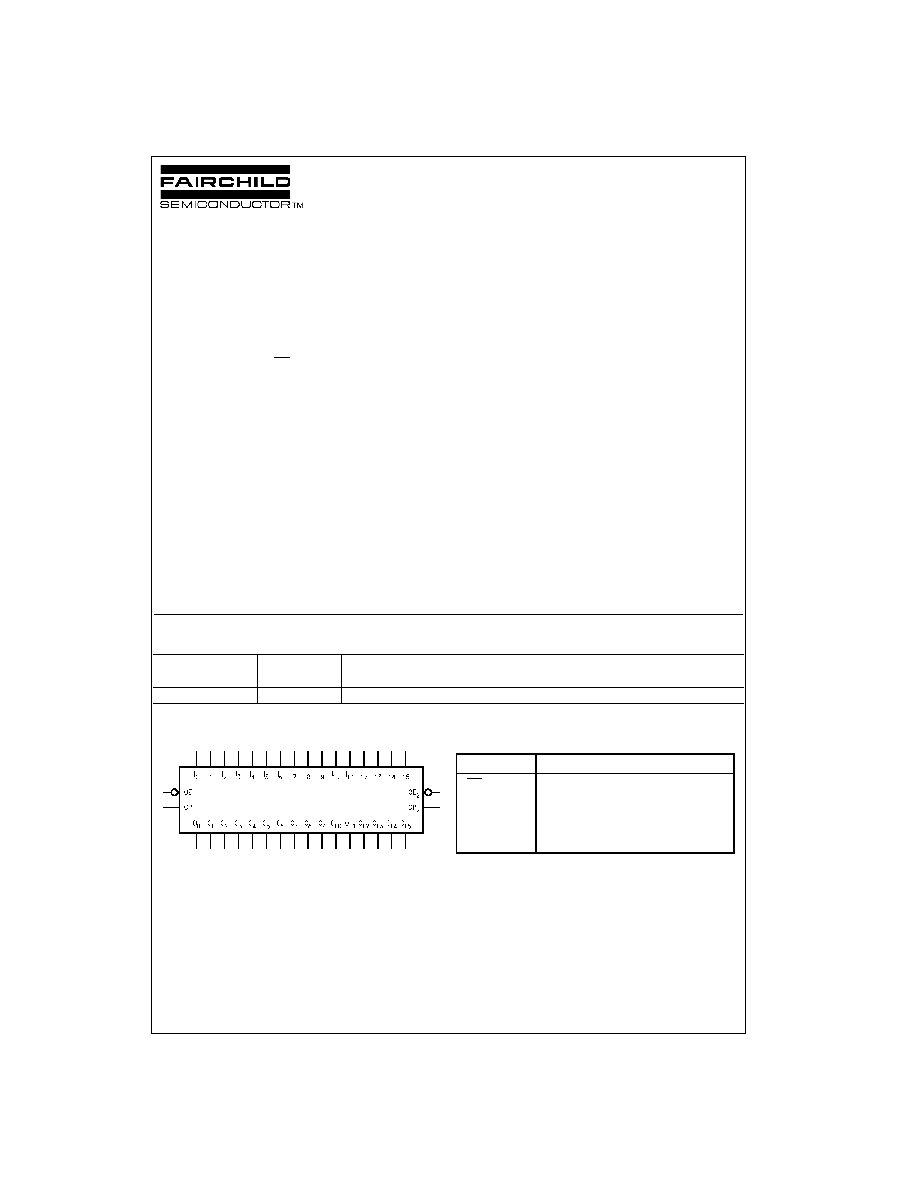
Logic Symbol
Pin Descriptions
Order Number
Package
Package Descriptions
Number
74VCXH16374MTD
MTD48
48-Lead Thin Shrink Small Outline Package (TSSOP), JEDEC MO-153, 6.1mm Wide
Pin Names
Description
OE
n
Output Enable Input (Active LOW)
CP
n
Clock Pulse Input
I
0
≠I
15
Bushold Inputs
O
0
≠O
15
Outputs
www.fairchildsemi.com
2
74VCXH16374
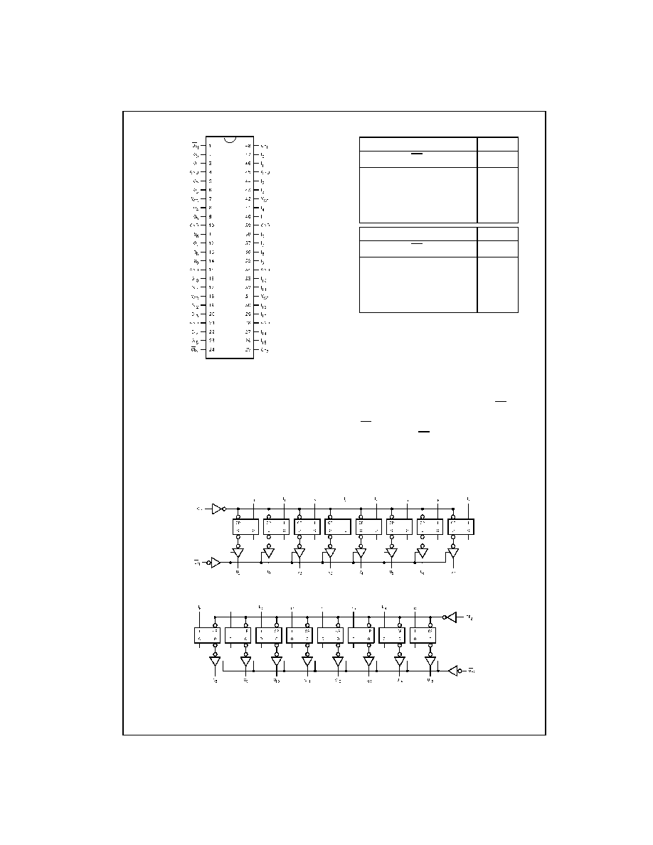
Connection Diagram
Truth Tables
H
=
HIGH Voltage Level
L
=
LOW Voltage Level
X
=
Immaterial (HIGH or LOW, control inputs may not float)
Z
=
High Impedance
O
0
=
Previous O
0
before HIGH-to-LOW of CP
Functional Description
The 74VCXH16374 consists of sixteen edge-triggered flip-
flops with individual D-type inputs and 3-STATE true out-
puts. The device is byte controlled with each byte function-
ing identically, but independent of the other. The control
pins can be shorted together to obtain full 16-bit operation.
Each clock has a buffered clock and buffered Output
Enable common to all flip-flops within that byte. The
description which follows applies to each byte. Each flip-
flop will store the state of their individual I inputs that meet
the setup and hold time requirements on the LOW-to-HIGH
Clock (CP
n
) transition. With the Output Enable (OE
n
) LOW,
the contents of the flip-flops are available at the outputs.
When OE
n
is HIGH, the outputs go to the high impedance
state. Operations of the OE
n
input does not affect the state
of the flip-flops.
Logic Diagram
Byte 1 (0:7)
Byte 2 (8:15)
Please note that this diagram is provided only for the understanding of logic operations and should not be used to estimate propagation delays.
Inputs
Outputs
CP
1
OE
1
I
0
≠I
7
O
0
≠O
7
L
H
H
L
L
L
L
L
X
O
0
X
H
X
Z
Inputs
Outputs
CP
2
OE
2
I
8
≠I
15
O
8
≠O
15
L
H
H
L
L
L
L
L
X
O
0
X
H
X
Z

3
www.fairchildsemi.com
7
4
VC
XH163
74
Absolute Maximum Ratings
(Note 1)
Recommended Operating
Conditions
(Note 3)
Note 1: The Absolute Maximum Ratings are those values beyond which
the safety of the device cannot be guaranteed. The device should not be
operated at these limits. The parametric values defined in the Electrical
Characteristics tables are not guaranteed at the Absolute Maximum Rat-
ings. The "Recommended Operating Conditions" table will define the condi-
tions for actual device operation.
Note 2: I
O
Absolute Maximum Rating must be observed.
Note 3: Floating or unused control inputs must be held HIGH or LOW.
DC Electrical Characteristics (2.7V
<
V
CC
3.6V)
Note 4: An external driver must source at least the specified current to switch from LOW-to-HIGH.
Note 5: An external driver must sink at least the specified current to switch from HIGH-to-LOW.
Note 6: Outputs disabled or 3-STATE only.
Supply Voltage (V
CC
)
-
0.5V to
+
4.6V
DC Input Voltage (V
I
)
OE
n
, CP
n
-
0.5V to 4.6V
I
0
≠ I
15
-
0.5V to V
CC
+
0.5V
Output Voltage (V
O
)
Outputs 3-STATED
-
0.5V to
+
4.6V
Outputs Active (Note 2)
-
0.5V to V
CC
+
0.5V
DC Input Diode Current (I
IK
)
V
I
<
0V
-
50 mA
DC Output Diode Current (I
OK
)
V
O
<
0V
-
50 mA
V
O
>
V
CC
+
50 mA
DC Output Source/Sink Current
(I
OH
/I
OL
)
±
50 mA
DC V
CC
or GND Current per
Supply Pin (I
CC
or GND)
±
100 mA
Storage Temperature Range (T
STG
)
-
65
∞
C to
+
150
∞
C
Power Supply
Operating
1.65V to 3.6V
Data Retention Only
1.2V to 3.6V
Input Voltage
-
0.3V to V
CC
Output Voltage (V
O
)
Output in Active States
0V to V
CC
Output in "OFF" State
0.0V to 3.6V
Output Current in I
OH
/I
OL
V
CC
=
3.0V to 3.6V
±
24 mA
V
CC
=
2.3V to 2.7V
±
18 mA
V
CC
=
1.65V to 2.3V
±
6 mA
Free Air Operating Temperature (T
A
)
-
40
∞
C to
+
85
∞
C
Minimum Input Edge Rate (
t/
V)
V
IN
=
0.8V to 2.0V, V
CC
=
3.0V
10 ns/V
Symbol
Parameter
Conditions
V
CC
(V)
Min
Max
Units
V
IH
HIGH Level Input Voltage
2.7
-
3.6
2.0
V
V
IL
LOW Level Input Voltage
2.7
-
3.6
0.8
V
V
OH
HIGH Level Output Voltage
I
OH
=
-
100
µ
A 2.7
-
3.6
V
CC
-
0.2
V
I
OH
=
-
12 mA
2.7
2.2
V
I
OH
=
-
18 mA
3.0
2.4
V
I
OH
=
-
24 mA
3.0
2.2
V
V
OL
LOW Level Output Voltage
I
OL
=
100
µ
A 2.7
-
3.6
0.2
V
I
OL
=
12 mA
2.7
0.4
V
I
OL
=
18 mA
3.0
0.4
V
I
OL
=
24 mA
3.0
0.55
V
I
I
Input Leakage Current
Control Pins
0
V
I
3.6V
2.7
-
3.6
±
5.0
µ
A
Data Pins
V
I
=
V
CC
or GND
2.7
-
3.6
±
5.0
µ
A
I
I(HOLD)
Bushold Input Minimum
V
IN
=
0.8V
3.0
75
µ
A
Drive Hold Current
V
IN
=
2.0V
3.0
-
75
I
I(OD)
Bushold Input Over-Drive
(Note 4)
3.6
450
µ
A
Current to Change State
(Note 5)
3.6
-
450
I
OZ
3-STATE Output Leakage
0
V
O
3.6V
2.7
-
3.6
±
10
µ
A
V
I
=
V
IH
or V
IL
I
OFF
Power-OFF Leakage Current
0
(V
O
)
3.6V
0
10
µ
A
I
CC
Quiescent Supply Current
V
I
=
V
CC
or GND
2.7
-
3.6
20
µ
A
V
CC
(V
O
)
3.6V (Note 6)
2.7
-
3.6
±
20
µ
A
I
CC
Increase in I
CC
per Input
V
IH
=
V
CC
-
0.6V
2.7
-
3.6
750
µ
A
www.fairchildsemi.com
4
74VCXH16374
DC Electrical Characteristics (2.3V
V
CC
2.7V)
Note 7: An external driver must source at least the specified current to switch from LOW-to-HIGH.
Note 8: An external driver must sink at least the specified current to switch from HIGH-to-LOW.
Note 9: Outputs disabled or 3-STATE only.
DC Electrical Characteristics (1.65V
V
CC
<
2.3V)
Note 10: An external driver must source at least the specified current to switch from LOW-to-HIGH.
Note 11: An external driver must sink at least the specified current to switch from HIGH-to-LOW.
Note 12: Outputs disabled or 3-STATE only.
Symbol
Parameter
Conditions
V
CC
(V)
Min
Max
Units
V
IH
HIGH Level Input Voltage
2.3
-
2.7
1.6
V
V
IL
LOW Level Input Voltage
2.3
-
2.7
0.7
V
V
OH
HIGH Level Output Voltage
I
OH
=
-
100
µ
A 2.3
-
2.7
V
CC
-
0.2
V
I
OH
=
-
6 mA
2.3
2.0
V
I
OH
=
-
12 mA
2.3
1.8
V
I
OH
=
-
18 mA
2.3
1.7
V
V
OL
LOW Level Output Voltage
I
OL
=
100
µ
A 2.3
-
2.7
0.2
V
I
OL
=
12 mA
2.3
0.4
V
I
OL
=
18 mA
2.3
0.6
V
I
I
Input Leakage Current
Control Pins
0
V
I
3.6V
2.3
-
2.7
±
5.0
µ
A
Data Pins
V
I
=
V
CC
or GND
2.3
-
2.7
±
5.0
µ
A
I
I(HOLD)
Bushold Input Minimum
V
IN
=
0.7V
2.3
45
µ
A
Drive Hold Current
V
IN
=
1.6V
2.3
-45
I
I(OD)
Bushold Input Over-Drive
(Note 7)
2.7
300
µ
A
Current to Change State
(Note 8)
2.7
-
300
I
OZ
3-STATE Output Leakage
0
V
O
3.6V
2.3
-
2.7
±
10
µ
A
V
I
=
V
IH
or V
IL
I
OFF
Power-OFF Leakage Current
0
(V
O
)
3.6V
0
10
µ
A
I
CC
Quiescent Supply Current
V
I
=
V
CC
or GND
2.3
-
2.7
20
µ
A
V
CC
(V
O
)
3.6V (Note 9)
2.3
-
2.7
±
20
µ
A
Symbol
Parameter
Conditions
V
CC
(V)
Min
Max
Units
V
IH
HIGH Level Input Voltage
1.65 - 2.3
0.65
◊
V
CC
V
V
IL
LOW Level Input Voltage
1.65 - 2.3
0.35
◊
V
CC
V
V
OH
HIGH Level Output Voltage
I
OH
=
-
100
µ
A
1.65 - 2.3
V
CC
-
0.2
V
I
OH
=
-
6 mA
1.65
1.25
V
V
OL
LOW Level Output Voltage
I
OL
=
100
µ
A
1.65 - 2.3
0.2
V
I
OL
=
6 mA
1.65
0.3
V
I
I
Input Leakage Current
Control Pins
0
V
I
3.6V
1.65 - 2.3
±
5.0
µ
A
Data Pins
V
I
=
V
CC
or GND
1.65 - 2.3
±
5.0
µ
A
I
I(HOLD)
Bushold Input Minimum
V
IN
=
0.57V
1.65
25
µ
A
Drive Hold Current
V
IN
=
1.07V
1.65
-25
I
I(OD)
Bushold Input Over-Drive
(Note 10)
1.95
200
µ
A
Current to Change State
(Note 11)
1.95
-
200
I
OZ
3-STATE Output Leakage
0
V
O
3.6V
1.65 - 2.3
±
10
µ
A
V
I
=
V
IH
or V
IL
I
OFF
Power-OFF Leakage Current
0
(V
O
)
3.6V
0
10
µ
A
I
CC
Quiescent Supply Current
V
I
=
V
CC
or GND
1.65 - 2.3
20
µ
A
V
CC
(V
O
)
3.6V (Note 12)
1.65 - 2.3
±
20
µ
A

5
www.fairchildsemi.com
7
4
VC
XH163
74
AC Electrical Characteristics
(Note 13)
Note 13: For C
L
=
50
P
F, add approximately 300 ps to the AC maximum specification.
Note 14: Skew is defined as the absolute value of the difference between the actual propagation delay for any two separate outputs of the same device. The
specification applies to any outputs switching in the same direction, either HIGH-to-LOW (t
OSHL
) or LOW-to-HIGH (t
OSLH
).
Dynamic Switching Characteristics
Capacitance
Symbol
Parameter
T
A
=
-
40
∞
C to
+
85
∞
C, C
L
=
30 pF, R
L
=
500
Units
V
CC
=
3.3V
±
0.3V
V
CC
=
2.5V
±
0.2V
V
CC
=
1.8V
±
0.15V
Min
Max
Min
Max
Min
Max
f
MAX
Maximum Clock Frequency
250
200
100
MHz
t
PHL
, t
PLH
Prop Delay CP to O
n
0.8
3.0
1.0
3.9
1.5
7.8
ns
t
PZL
, t
PZH
Output Enable Time
0.8
3.5
1.0
4.6
1.5
9.2
ns
t
PLZ
, t
PHZ
Output Disable Time
0.8
3.5
1.0
3.8
1.5
6.8
ns
t
S
Setup Time
1.5
1.5
2.5
ns
t
H
Hold Time
1.0
1.0
1.0
ns
t
W
Pulse Width
1.5
1.5
4.0
ns
t
OSHL
Output to Output Skew
0.5
0.5
0.75
ns
t
OSLH
(Note 14)
Symbol
Parameter
Conditions
V
CC
(V)
T
A
=
+
25
∞
C
Units
Typical
V
OLP
Quiet Output Dynamic Peak V
OL
C
L
=
30 pF, V
IH
=
V
CC
, V
IL
=
0V
1.8
0.25
V
2.5
0.6
3.3
0.8
V
OLV
Quiet Output Dynamic Valley V
OL
C
L
=
30 pF, V
IH
=
V
CC
, V
IL
=
0V
1.8
-
0.25
V
2.5
-
0.6
3.3
-
0.8
V
OHV
Quiet Output Dynamic Valley V
OH
C
L
=
30 pF, V
IH
=
V
CC
, V
IL
=
0V
1.8
1.5
V
2.5
1.9
3.3
2.2
Symbol
Parameter
Conditions
T
A
=
+
25
∞
C
Units
Typical
C
IN
Input Capacitance
V
CC
=
1.8V, 2.5V or 3.3V, V
I
=
0V or V
CC
6
pF
C
OUT
Output Capacitance
V
I
=
0V or V
CC
, V
CC
=
1.8V, 2.5V or 3.3V
7
pF
C
PD
Power Dissipation Capacitance
V
I
=
0V or V
CC
, f
=
10 MHz,
20
pF
V
CC
=
1.8V, 2.5V or 3.3V
www.fairchildsemi.com
6
74VCXH16374
AC Loading and Waveforms
FIGURE 1. AC Test Circuit
FIGURE 2. Waveform for Inverting and
Non-Inverting Functions
FIGURE 3. 3-STATE Output High Enable and
Disable Times for Low Voltage Logic
FIGURE 4. 3-STATE Output Low Enable and Disable Times for Low Voltage Logic
FIGURE 5. Propagation Delay, Pulse Width and
t
REC
Waveforms
FIGURE 6. Setup Time, Hold Time and
Recovery Time for Low Voltage Logic
TEST
SWITCH
t
PLH
, t
PHL
Open
t
PZL
, t
PLZ
6V at V
CC
=
3.3
±
0.3V;
V
CC
x 2 at V
CC
=
2.5
±
0.2V; 1.8V
±
0.15V
t
PZH
, t
PHZ
GND
Symbol
V
CC
3.3V
±
0.3V
2.5V
±
0.2V
1.8V
±
0.15V
V
mi
1.5V
V
CC
/2
V
CC
/2
V
mo
1.5V
V
CC
/2
V
CC
/2
V
X
V
OL
+
0.3V
V
OL
+
0.15V V
OL
+
0.15V
V
Y
V
OH
-
0.3V V
OH
-
0.15V V
OH
-
0.15V
7
www.fairchildsemi.com
7
4
VC
XH163
74
Low V
o
l
t
age
16
-Bit
D
-
T
ype Fli
p
-Fl
op w
i
th Bushol
d
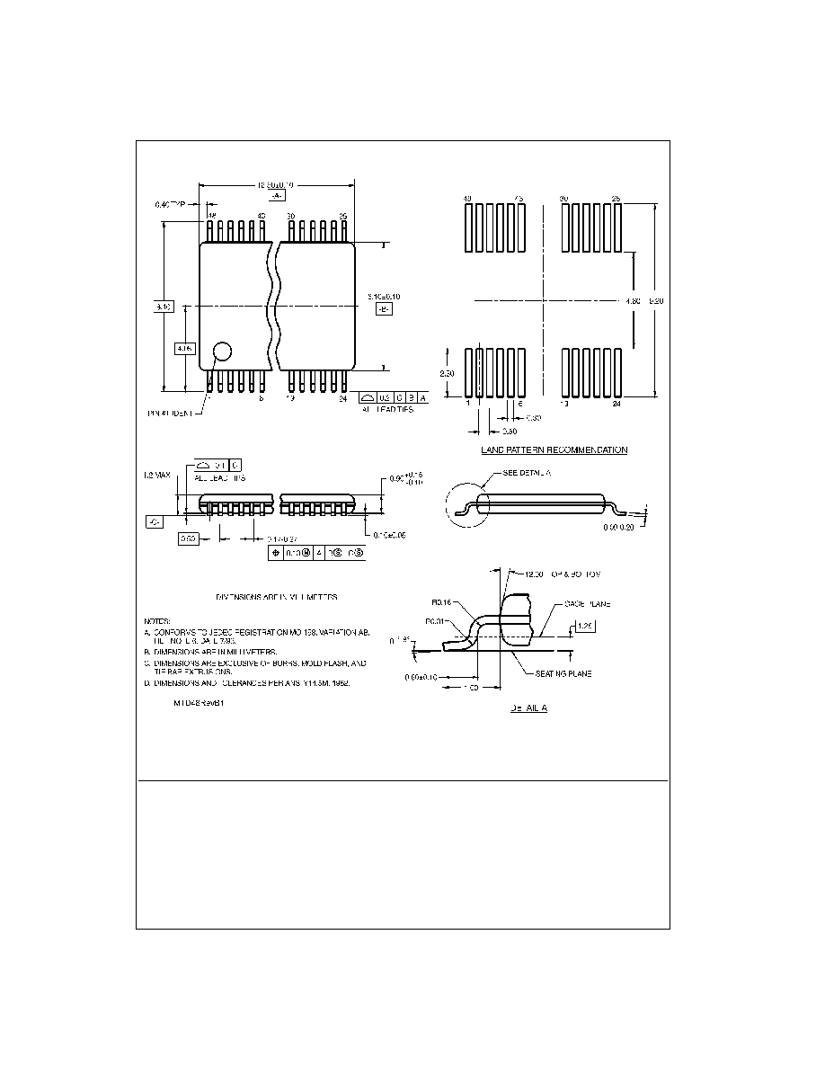
Physical Dimensions
inches (millimeters) unless otherwise noted
48-Lead Thin Shrink Small Outline Package (TSSOP), JEDEC MO-153, 6.1mm Body Width
Package Number MTD48
Fairchild does not assume any responsibility for use of any circuitry described, no circuit patent licenses are implied and
Fairchild reserves the right at any time without notice to change said circuitry and specifications.
LIFE SUPPORT POLICY
FAIRCHILD'S PRODUCTS ARE NOT AUTHORIZED FOR USE AS CRITICAL COMPONENTS IN LIFE SUPPORT
DEVICES OR SYSTEMS WITHOUT THE EXPRESS WRITTEN APPROVAL OF THE PRESIDENT OF FAIRCHILD
SEMICONDUCTOR CORPORATION. As used herein:
1. Life support devices or systems are devices or systems
which, (a) are intended for surgical implant into the
body, or (b) support or sustain life, and (c) whose failure
to perform when properly used in accordance with
instructions for use provided in the labeling, can be rea-
sonably expected to result in a significant injury to the
user.
2. A critical component in any component of a life support
device or system whose failure to perform can be rea-
sonably expected to cause the failure of the life support
device or system, or to affect its safety or effectiveness.
www.fairchildsemi.com