November 1992
Revised April 1999
7
4
VH
C13
8
3-
to-
8
D
e
c
oder/
D
em
ul
ti
pl
exer
© 1999 Fairchild Semiconductor Corporation
DS011537.prf
www.fairchildsemi.com
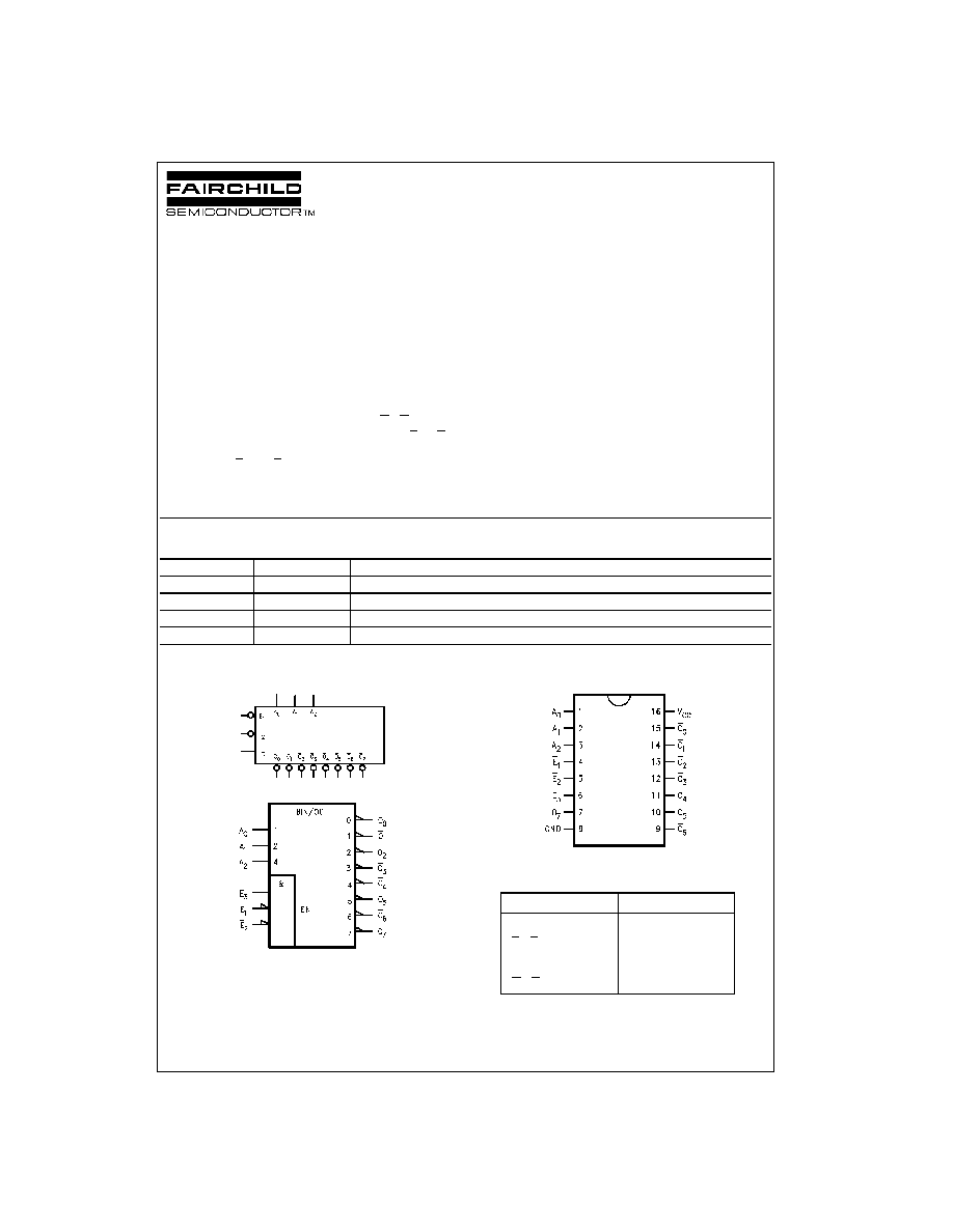
74VHC138
3-to-8 Decoder/Demultiplexer
General Description
The VHC138 is an advanced high speed CMOS 3-to-8
decoder/demultiplexer fabricated with silicon gate CMOS
technology. It achieves the high speed operation similar to
equivalent Bipolar Schottky TTL while maintaining the
CMOS low power dissipation.
When the device is enabled, 3 binary select inputs (A
0
, A
1
and A
2
) determine which one of the outputs (O
0
≠O
7
) will go
LOW. When enable input E
3
is held LOW or either E
1
or E
2
is held HIGH, decoding function is inhibited and all outputs
go HIGH. E
3
, E
1
and E
2
inputs are provided to ease cas-
cade connection and for use as an address decoder for
memory systems. An input protection circuit ensures that
0V to 7V can be applied to the input pins without regard to
the supply voltage. This device can be used to interface 5V
to 3V systems and two supply systems such as battery
back up. This circuit prevents device destruction due to
mismatched supply and input voltages.
Features
s
High Speed: t
PD
=
5.7ns (typ) at T
A
=
25
∞
C
s
Low power dissipation: I
CC
=
4
µ
A (max.) at T
A
=
25
∞
C
s
High noise immunity: V
NIH
=
V
NIL
=
28% V
CC
(min.)
s
Power down protection provided on all inputs
s
Pin and function compatible with 74HC138
Ordering Code:
Surface mount packages are also available on Tape and Reel. Specify by appending the suffix letter "X" to the ordering code.
Logic Symbols
IEEE/IEC
Connection Diagram
Pin Descriptions
Order Number
Package Number
Package Description
74VHC138M
M16A
16-Lead Small Outline Integrated Circuit (SOIC), JEDEC MS-012, 0.150" Narrow
74VHC138SJ
M16D
16-Lead Small Outline Package (SOP), EIAJ TYPE II, 5.3mm Wide
74VHC138MTC
MTC16
16-Lead Thin Shrink Small Outline Package (TSSOP), JEDEC MO-153, 4.4mm Wide
74VHC138N
N16E
16-Lead Plastic Dual-In-Line Package (PDIP), JEDEC MS-001, 0.300" Wide
Pin Names
Description
A
0
≠A
2
Address Inputs
E
1
≠E
2
Enable Inputs
E
3
Enable Input
O
0
≠O
7
Outputs
3
www.fairchildsemi.com
7
4
VH
C13
8
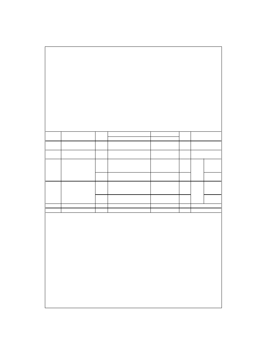
Absolute Maximum Ratings
(Note 1)
Recommended Operating
Conditions
(Note 2)
Note 1: Absolute Maximum Ratings are values beyond which the device
may be damaged or have its useful life impaired. The databook specifica-
tions should be met, without exception, to ensure that the system design is
reliable over its power supply, temperature, and output/input loading vari-
ables. Fairchild does not recommend operation outside databook specifica-
tions.
Note 2: Unused inputs must be held HIGH or LOW. They may not float.
DC Electrical Characteristics
Supply Voltage (V
CC
)
-
0.5V to
+
7.0V
DC Input Voltage (V
IN
)
-
0.5V to
+
7.0V
DC Output Voltage (V
OUT
)
-
0.5V to V
CC
+
0.5V
Input Diode Current (I
IK
)
-
20 mA
Output Diode Current (I
OK
)
±
20 mA
DC Output Current (I
OUT
)
±
25 mA
DC V
CC
/GND Current (I
CC
)
±
75 mA
Storage Temperature (T
STG
)
-
65
∞
C to
+
150
∞
C
Lead Temperature (T
L
)
(Soldering, 10 seconds)
260
∞
C
Supply Voltage (V
CC
)
2.0V to
+
5.5V
Input Voltage (V
IN
)
0V to
+
5.5V
Output Voltage (V
OUT
)
0V to V
CC
Operating Temperature (T
OPR
)
-
40
∞
C to
+
85
∞
C
Input Rise and Fall Time (t
r
, t
f
)
V
CC
=
3.3V
±
0.3V
0
100 ns/V
V
CC
=
5.0V
±
0.5V
0
20 ns/V
Symbol
Parameter
V
CC
(V)
T
A
=
25
∞
C
T
A
=
-
40
∞
C to
+
85
∞
C
Units
Conditions
Min
Typ
Max
Min
Max
V
IH
HIGH Level Input Voltage
2.0
1.50
1.50
V
3.0
-
5.5
0.7 V
CC
0.7 V
CC
V
IL
LOW Level Input Voltage
2.0
0.50
0.50
V
3.0
-
5.5
0.3 V
CC
0.3 V
CC
V
OH
HIGH Level Output Voltage
2.0
1.9
2.0
1.9
V
IN
=
V
IH
I
OH
=
-
50
µ
A
3.0
2.9
3.0
2.9
V
or V
IL
4.5
4.4
4.5
4.4
3.0
2.58
2.48
V
I
OH
=
-
4 mA
4.5
3.94
3.80
I
OH
=
-
8 mA
V
OL
LOW Level Output Voltage
2.0
0.0
0.1
0.1
V
IN
=
V
IH
I
OL
=
50
µ
A
3.0
0.0
0.1
0.1
V
or V
IL
4.5
0.0
0.1
0.1
3.0
0.36
0.44
V
I
OL
=
4 mA
4.5
0.36
0.44
I
OL
=
8 mA
I
IN
Input Leakage Current
0
-
5.5
±
0.1
±
1.0
µ
A
V
IN
=
5.5V or GND
I
CC
Quiescent Supply Current
5.5
4.0
40.0
µ
A
V
IN
=
V
CC
or GND
www.fairchildsemi.com
4
74
V
HC138
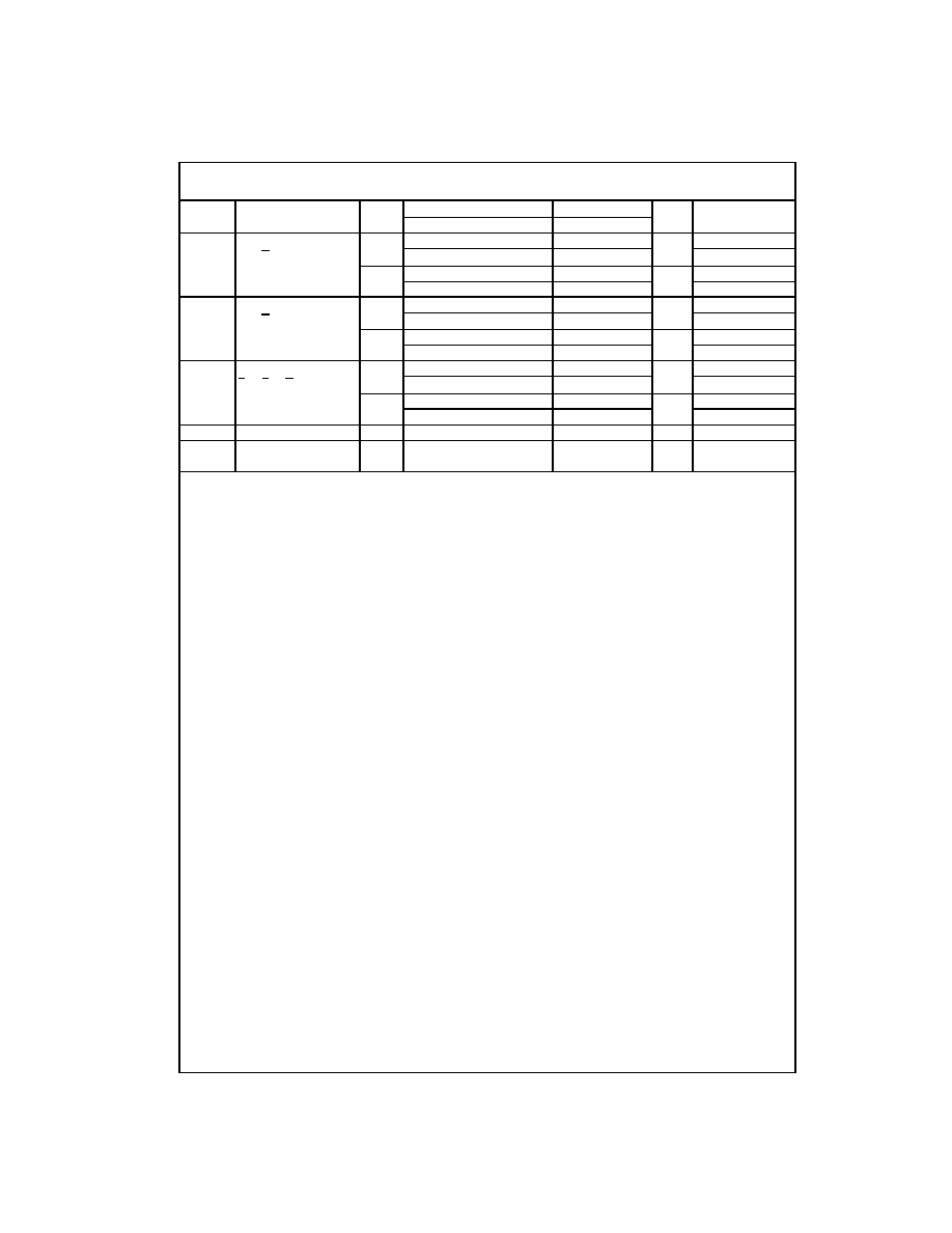
AC Electrical Characteristics
Note 3: C
PD
is defined as the value of the internal equivalent capacitance which is calculated from the operating current consumption without load. Average
operating current can be obtained by the equation: I
CC
(opr.)
=
C
PD
* V
CC
* f
IN
+
I
CC
.
Symbol
Parameter
V
CC
(V)
T
A
=
25
∞
C
T
A
=
-
40
∞
C to
+
85
∞
C
Units
Conditions
Min
Typ
Max
Min
Max
t
PLH
Propagation Delay
3.3
±
0.3
8.2
11.4
1.0
13.5
ns
C
L
=
15 pF
t
PHL
A
n
to O
n
10.0
15.8
1.0
18.0
C
L
=
50 pF
5.0
±
0.5
5.7
8.1
1.0
9.5
ns
C
L
=
15 pF
7.2
10.1
1.0
11.5
C
L
=
50 pF
t
PLH
Propagation Delay
3.3
±
0.3
8.1
12.8
1.0
15.0
ns
C
L
=
15 pF
t
PHL
E
3
to O
n
10.6
16.3
1.0
18.5
C
L
=
50 pF
5.0
±
0.5
5.6
8.1
1.0
9.5
ns
C
L
=
15 pF
7.1
10.1
1.0
11.5
C
L
=
50 pF
t
PLH
Propagation Delay
3.3
±
0.3
8.2
11.4
1.0
13.5
ns
C
L
=
15 pF
t
PHL
E
1
or E
2
to O
n
10.7
14.9
1.0
17.0
C
L
=
50 pF
5.0
±
0.5
5.8
8.1
1.0
9.5
ns
C
L
=
15 pF
7.3
10.1
1.0
11.5
C
L
=
50 pF
C
IN
Input Capacitance
4
10
10
pF
V
CC
=
Open
C
PD
Power Dissipation
34
pF
(Note 3)
Capacitance
5
www.fairchildsemi.com
7
4
VH
C13
8
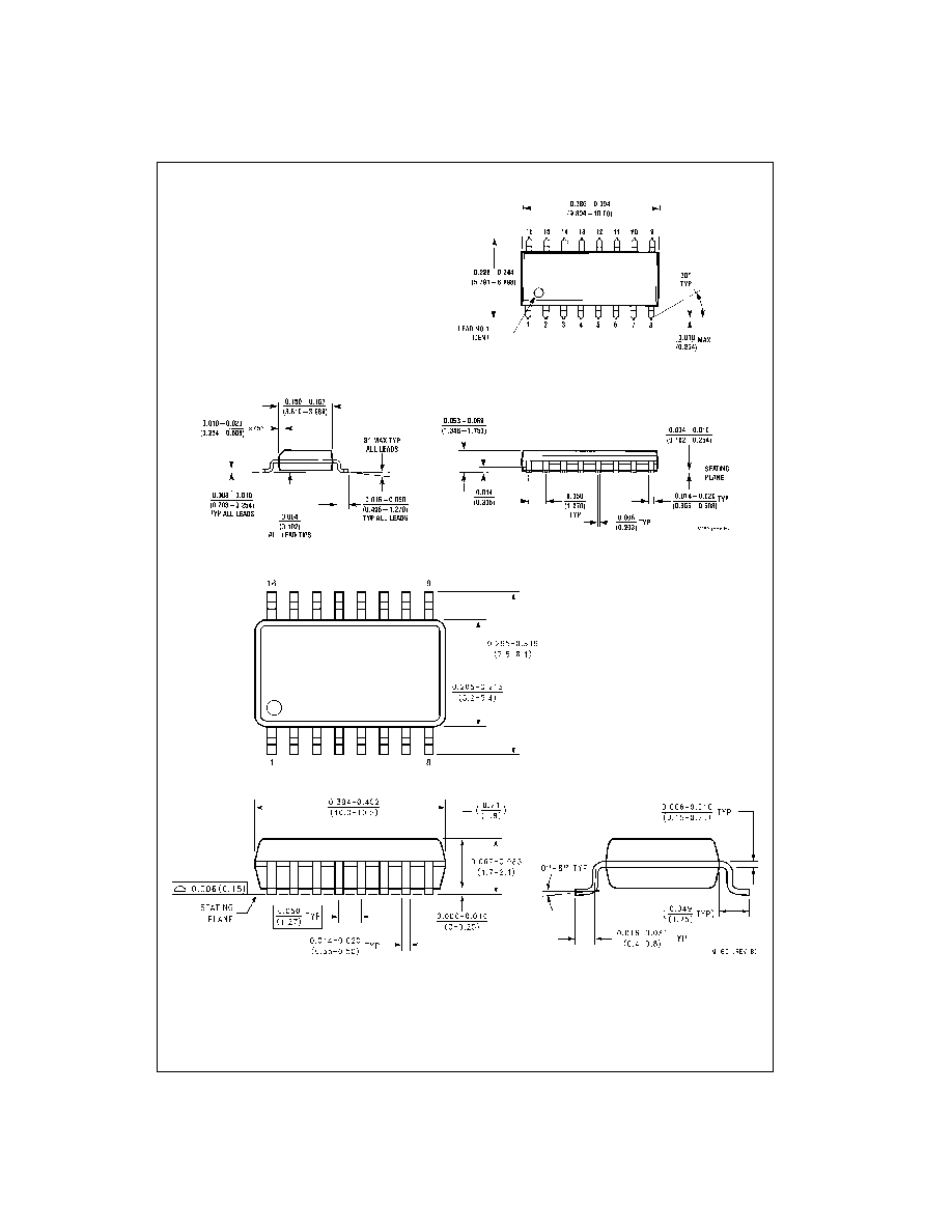
Physical Dimensions
inches (millimeters) unless otherwise noted
16-Lead Small Outline Integrated Circuit (SOIC), JEDEC MS-012, 0.150" Narrow
Package Number M16A
16-Lead Small Outline Package (SOP) EIAJ TYPE II, 5.3mm Wide
Package Number M16D