 | –≠–ª–µ–∫—Ç—Ä–æ–Ω–Ω—ã–π –∫–æ–º–ø–æ–Ω–µ–Ω—Ç: 74VHC163 | –°–∫–∞—á–∞—Ç—å:  PDF PDF  ZIP ZIP |

© 2002 Fairchild Semiconductor Corporation
DS012122
www.fairchildsemi.com
September 1995
Revised February 2002
7
4
VH
C16
3
4-
Bit
Bi
nary Counte
r
w
i
th Synchr
onous
Cl
ear
74VHC163
4-Bit Binary Counter with Synchronous Clear
General Description
The VHC163 is an advanced high-speed CMOS device
fabricated with silicon gate CMOS technology. It achieves
the high-speed operation similar to equivalent Bipolar
Schottky TTL while maintaining the CMOS low power dissi-
pation.
The VHC163 is a high-speed synchronous modulo-16
binary counter. This device is synchronously presettable for
application in programmable dividers and has two types of
Count Enable inputs plus a Terminal Count output for ver-
satility in forming multistage counters. The CLK input is
active on the rising edge. Both PE and MR inputs are
active on low logic level. Presetting is synchronous to rising
edge of CLK and the Clear function of the VHC163 is syn-
chronous to CLK. Two enable inputs (ENP and ENT) and
Carry Output are provided to enable easy cascading of
counters, which facilitates easy implementation of n-bit
counters without using external gates.
An input protection circuit insures that 0V to 7V can be
applied to the input pins without regard to the supply volt-
age. This device can be used to interface 5V to 3V systems
and two supply systems such as battery backup. This cir-
cuit prevents device destruction due to mismatched supply
and input voltages.
Features
s
High speed: f
MAX
=
185 MHz (typ) at V
CC
=
5V
s
Low power dissipation: I
CC
=
4
µ
A (max) at T
A
=
25
∞
C
s
Synchronous counting and loading
s
High-speed synchronous expansion
s
High noise immunity: V
NIH
=
V
NIL
=
28% V
CC
(min)
s
Power down protection is provided on all inputs.
s
Low noise: V
OLP
=
0.8V (max)
s
Pin and function compatible with 74HC163
Ordering Code:
Surface mount packages are also available on Tape and Reel. Specify by appending the suffix letter "X" to the ordering code.
Logic Symbols
IEEE/IEC
Order Number
Package Number
Package Description
74VHC163M
M16A
16-Lead Small Outline Integrated Circuit (SOIC), JEDEC MS-012, 0.150" Narrow
74VHC163SJ
M16D
16-Lead Small Outline Package (SOP), EIAJ TYPE II, 5.3mm Wide
74VHC163MTC
MTC16
16-Lead Thin Shrink Small Outline Package (TSSOP), JEDEC MO-153, 4.4mm Wide
74VHC163N
N16E
16-Lead Plastic Dual-In-Line Package (PDIP), JEDEC MS-001, 0.300" Wide
www.fairchildsemi.com
2
74
V
HC163
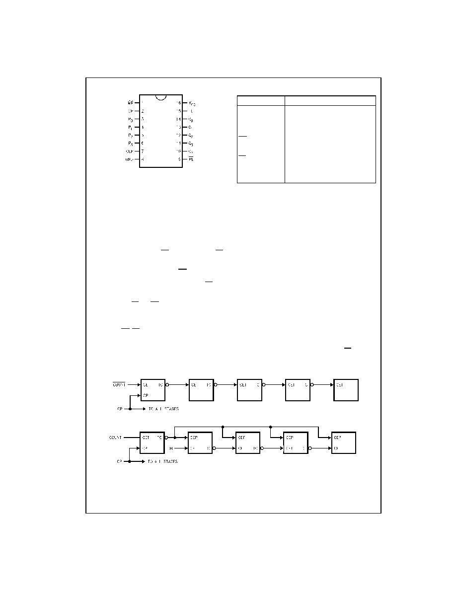
Connection Diagram
Pin Descriptions
Functional Description
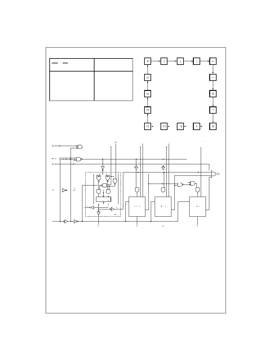
The VHC163 counts in modulo-16 binary sequence. From
state 15 (HHHH) it increments to state 0 (LLLL). The clock
inputs of all flip-flops are driven in parallel through a clock
buffer. Thus all changes of the Q outputs occur as a result
of, and synchronous with, the LOW-to-HIGH transition of
the CP input signal. The circuits have four fundamental
modes of operation, in order of precedence: synchronous
reset, parallel load, count-up and hold. Four control
inputs--Synchronous Reset (MR), Parallel Enable (PE),
Count Enable Parallel (CEP) and Count Enable Trickle
(CET)--determine the mode of operation, as shown in the
Mode Select Table. A LOW signal on MR overrides count-
ing and parallel loading and allows all outputs to go LOW
on the next rising edge of CP. A LOW signal on PE over-
rides counting and allows information on the Parallel Data
(P
n
) inputs to be loaded into the flip-flops on the next rising
edge of CP. With PE and MR HIGH, CEP and CET permit
counting when both are HIGH. Conversely, a LOW signal
on either CEP or CET inhibits counting.
The VHC163 uses D-type edge-triggered flip-flops and
changing the MR, PE, CEP and CET inputs when the CP is
in either state does not cause errors, provided that the rec-
ommended setup and hold times, with respect to the rising
edge of CP, are observed.
The Terminal Count (TC) output is HIGH when CET is
HIGH and counter is in state 15. To implement synchro-
nous multistage counters, the TC outputs can be used with
the CEP and CET inputs in two different ways.
Figure 1 shows the connections for simple ripple carry, in
which the clock period must be longer than the CP to TC
delay of the first stage, plus the cumulative CET to TC
delays of the intermediate stages, plus the CET to CP
setup time of the last stage. This total delay plus setup time
sets the upper limit on clock frequency. For faster clock
rates, the carry lookahead connections shown in Figure 2
are recommended. In this scheme the ripple delay through
the intermediate stages commences with the same clock
that causes the first stage to tick over from max to min to
start its final cycle. Since this final cycle takes 16 clocks to
complete, there is plenty of time for the ripple to progress
through the intermediate stages. The critical timing that lim-
its the clock period is the CP to TC delay of the first stage
plus the CEP to CP setup time of the last stage. The TC
output is subject to decoding spikes due to internal race
conditions and is therefore not recommended for use as a
clock or asynchronous reset for flip-flops, registers or
counters.
Logic Equations: Count Enable
=
CEP ∑ CET ∑ PE
TC
=
Q
0
∑ Q
1
∑ Q
2
∑ Q
3
∑ CET
FIGURE 1.
FIGURE 2.
Pin Names
Description
CEP
Count Enable Parallel Input
CET
Count Enable Trickle Input
CP
Clock Pulse Input
MR
Synchronous Master Reset Input
P
0
≠P
3
Parallel Data Inputs
PE
Parallel Enable Inputs
Q
0
≠Q
3
Flip-Flop Outputs
TC
Terminal Count Output
3
www.fairchildsemi.com
74
V
H
C
1
63
Mode Select Table
H
=
HIGH Voltage Level
L
=
LOW Voltage Level
X
=
Immaterial
State Diagram
Block Diagram
MR
PE
CET
CEP
Action on the Rising
Clock Edge (
)
L
X
X
X
Reset (Clear)
H
L
X
X
Load (P
n
Q
n
)
H
H
H
H
Count (Increment)
H
H
L
X
No Change (Hold)
H
H
X
L
No Change (Hold)
www.fairchildsemi.com
4
74
V
HC163
Absolute Maximum Ratings
(Note 1)
Recommended Operating
Conditions
(Note 2)
Note 1: Absolute Maximum Ratings are values beyond which the device
may be damaged or have its useful life impaired. The databook specifica-
tions should be met, without exception, to ensure that the system design is
reliable over its power supply, temperature, and output/input loading vari-
ables. Fairchild does not recommend operation outside databook specifica-
tions.
Note 2: Unused inputs must be held HIGH or LOW. They may not float.
DC Electrical Characteristics
Noise Characteristics
Note 3: Parameter guaranteed by design.
Supply Voltage (V
CC
)
-
0.5V to
+
7.0V
DC Input Voltage (V
IN
)
-
0.5V to
+
7.0V
DC Output Voltage (V
OUT
)
-
0.5V to V
CC
+
0.5V
Input Diode Current (I
IK
)
-
20 mA
Output Diode Current (I
OK
)
±
20 mA
DC Output Current (I
OUT
)
±
25 mA
DC V
CC
/GND Current (I
CC
)
±
50 mA
Storage Temperature (T
STG
)
-
65
∞
C to
+
150
∞
C
Lead Temperature (T
L
)
(Soldering, 10 seconds)
260
∞
C
Supply Voltage (V
CC
)
2.0V to
+
5.5V
Input Voltage (V
IN
)
0V to
+
5.5V
Output Voltage (V
OUT
)
0V to V
CC
Operating Temperature (T
OPR
)
-
40
∞
C to
+
85
∞
C
Input Rise and Fall Time (t
r
, t
f
)
V
CC
=
3.3V
±
0.3V
0
100 ns/V
V
CC
=
5.0V
±
0.5V
0
20 ns/V
Symbol
Parameter
V
CC
T
A
=
25
∞
C
T
A
=
-
40
∞
C to
+
85
∞
C
Units
Conditions
(V)
Min
Typ
Max
Min
Max
V
IH
HIGH Level
2.0
1.50
1.50
V
Input Voltage
3.0
-
5.5
0.7 V
CC
0.7 V
CC
V
IL
LOW Level
2.0
0.50
0.50
V
Input Voltage
3.0
-
5.5
0.3 V
CC
0.3 V
CC
V
OH
HIGH Level
2.0
1.9
2.0
1.9
Output Voltage
3.0
2.9
3.0
2.9
V
I
OH
=
-
50
µ
A
4.5
4.4
4.5
4.4
V
IN
=
V
IH
3.0
2.58
2.48
V
or V
IL
I
OH
=
-
4 mA
4.5
3.94
3.80
I
OH
=
-
8 mA
V
OL
LOW Level
2.0
0.0
0.1
0.1
Output Voltage
3.0
0.0
0.1
0.1
V
I
OL
=
50
µ
A
4.5
0.0
0.1
0.1
V
IN
=
V
IH
3.0
0.36
0.44
V
or V
IL
I
OL
=
4 mA
4.5
0.36
0.44
I
OL
=
8 mA
I
IN
Input Leakage Current
0
-
5.5
±
0.1
±
1.0
µ
A
V
IN
=
5.5V or GND
I
CC
Quiescent Supply Current
5.5
4.0
40.0
µ
A
V
IN
=
V
CC
or GND
Symbol
Parameter
V
CC
T
A
=
25
∞
C
Units
Conditions
(V)
Typ
Limits
V
OLP
Quiet Output Maximum
5.0
0.4
0.8
V
C
L
=
50 pF
(Note 3)
Dynamic V
OL
V
OLV
Quiet Output Minimum
5.0
-
0.4
-
0.8
V
C
L
=
50 pF
(Note 3)
Dynamic V
OL
V
IHD
Minimum HIGH Level
5.0
3.5
V
C
L
=
50 pF
(Note 3)
Dynamic Input Voltage
V
ILD
Maximum LOW Level
5.0
1.5
V
C
L
=
50 pF
(Note 3)
Dynamic Input Voltage
5
www.fairchildsemi.com
74
V
H
C
1
63
AC Electrical Characteristics
Note 4: C
PD
is defined as the value of the internal equivalent capacitance which is calculated from the operating current consumption without load. Average
operating current can be obtained by the equation: I
CC
(opr)
=
C
PD
* V
CC
* f
IN
+
I
CC
.
When the outputs drive a capacitive load, total current consumption is the sum of C
PD
, and
I
CC
which is obtained from the following formula:
C
Q0
≠C
Q3
and C
TC
are the capacitances at Q0≠Q3 and TC, respectively. F
CP
is the input frequency of the CP.
Symbol
Parameter
V
CC
T
A
=
25
∞
C
T
A
=
-
40
∞
to
+
85
∞
C
Units
Conditions
(V)
Min
Typ
Max
Min
Max
t
PLH
Propagation Delay
3.3
±
0.3
8.3
12.8
1.0
15.0
ns
C
L
=
15 pF
t
PHL
Time (CP≠Q
n
)
10.8
16.3
1.0
18.5
C
L
=
50 pF
5.0
±
0.5
4.9
8.1
1.0
9.5
ns
C
L
=
15 pF
6.4
10.1
1.0
11.5
C
L
=
50 pF
t
PLH
Propagation Delay
3.3
±
0.3
8.7
13.6
1.0
16.0
ns
C
L
=
15 pF
t
PHL
Time (CP≠TC, Count)
11.2
17.1
1.0
19.5
C
L
=
50 pF
5.0
±
0.5
4.9
8.1
1.0
9.5
ns
C
L
=
15 pF
6.4
10.1
1.0
11.5
C
L
=
50 pF
t
PLH
Propagation Delay
3.3
±
0.3
11.0
17.2
1.0
20.0
ns
C
L
=
15 pF
t
PHL
Time (CP≠TC, Load)
13.5
20.7
1.0
23.5
C
L
=
50 pF
5.0
±
0.5
6.2
10.3
1.0
12.0
ns
C
L
=
15 pF
7.7
12.3
1.0
14.0
C
L
=
50 pF
t
PLH
Propagation Delay
3.3
±
0.3
7.5
12.3
1.0
14.5
ns
C
L
=
15 pF
t
PHL
Time (CET≠TC)
10.5
15.8
1.0
18.0
C
L
=
50 pF
5.0
±
0.5
4.9
8.1
1.0
9.5
ns
C
L
=
15 pF
6.4
10.1
1.0
11.5
C
L
=
50 pF
f
MAX
Maximum Clock
3.3
±
0.3
80
130
70
MHz
C
L
=
15 pF
Frequency
55
85
50
C
L
=
50 pF
5.0
±
0.5
135
185
115
MHz
C
L
=
15 pF
95
125
85
C
L
=
50 pF
C
IN
Input Capacitance
4
10
10
pF
V
CC
=
Open
C
PD
Power Dissipation
23
pF
(Note 4)
Capacitance