
© 2005 Fairchild Semiconductor Corporation
DS011639
www.fairchildsemi.com
August 1993
Revised May 2005
7
4
VH
C54
1
Oct
a
l
Buf
f
er
/Li
ne Driv
er w
i
th 3-
ST
A
T
E O
u
t
put
s
74VHC541
Octal Buffer/Line Driver with 3-STATE Outputs
General Description
The VHC541 is an advanced high-speed CMOS device
fabricated with silicon gate CMOS technology. It achieves
the high-speed operation similar to equivalent Bipolar
Schottky TTL while maintaining the CMOS low power dissi-
pation.
The VHC541 is an octal buffer/line driver designed to be
employed as memory and address drivers, clock drivers
and bus oriented transmitter/receivers.
This device is similar in function to the VHC244 while pro-
viding flow-through architecture (inputs on opposite side
from outputs). This pinout arrangement makes this device
especially useful as an output port for microprocessors,
allowing ease of layout and greater PC board density.
An input protection circuit insures that 0V to 7V can be
applied to the input pins without regard to the supply volt-
age. This device can be used to interface 5V to 3V systems
and two supply systems such as battery backup. This cir-
cuit prevents device destruction due to mismatched supply
and input voltages.
Features
s
High Speed: t
PD
3.5 ns (typ) at V
CC
5V
s
Low power dissipation: I
CC
4
P
A (max) at T
A
25
q
C
s
High noise immunity: V
NIH
V
NIL
28% V
CC
(min)
s
Power down protection is provided on all inputs
s
Low noise: V
OLP
0.9V (typ)
s
Pin and function compatible with 74HC541
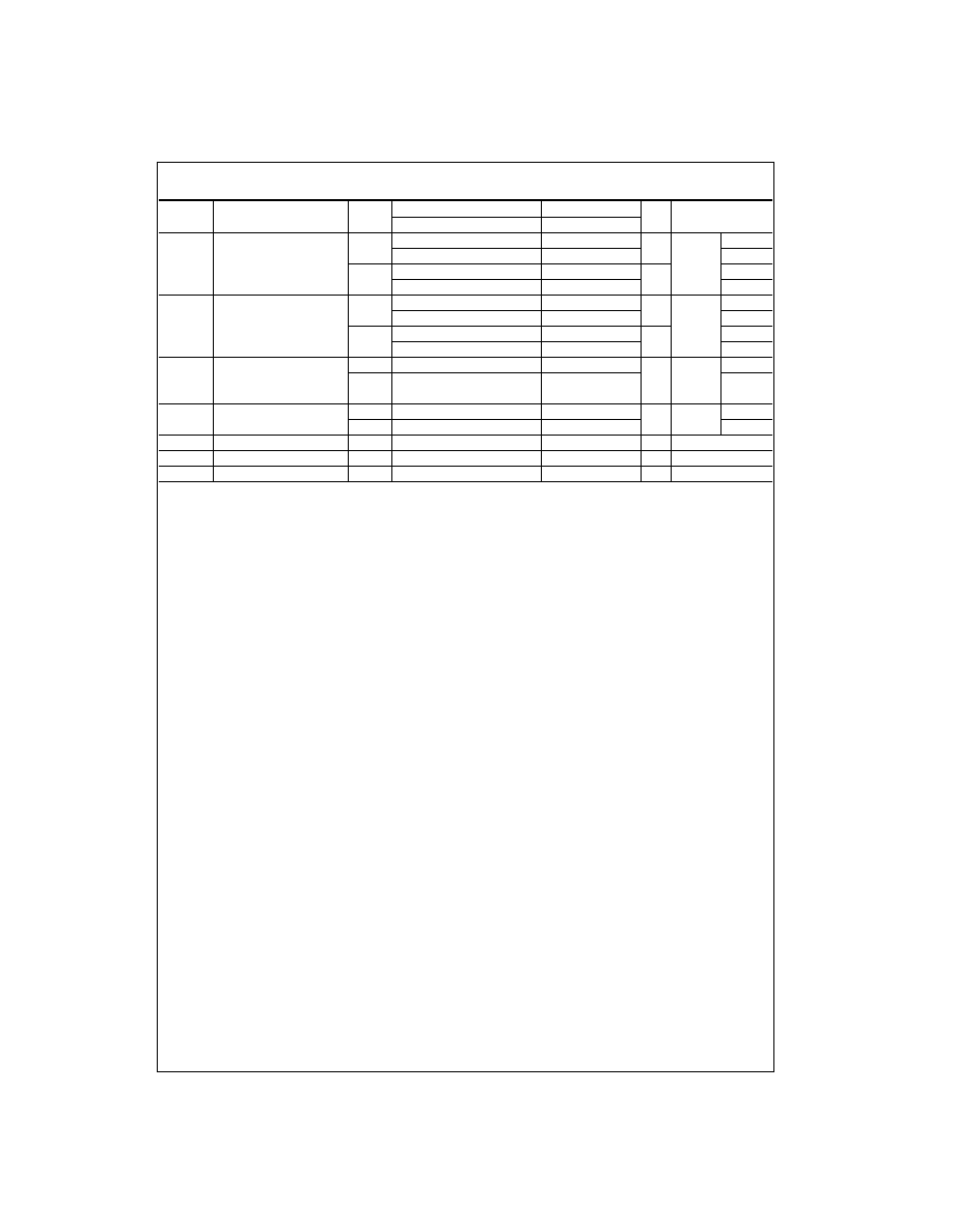
Ordering Code:
Surface mount packages are also available on Tape and Reel. Specify by appending the suffix letter "X" to the ordering code.
Pb-Free package per JEDEC J-STD-020B.
Connection Diagram
Pin Descriptions
Logic Symbol
IEEE/IEC
Truth Table
H
HIGH Voltage Level
X
Immaterial
L
LOW Voltage Level
Z
High Impedance
Order Number
Package Number
Package Description
74VHC541M
M20B
20-Lead Small Outline Integrated Circuit (SOIC), JEDEC MS-013, 0.300" Wide
74VHC541SJ
M20D
Pb-Free 20-Lead Small Outline Package (SOP), EIAJ TYPE II, 5.3mm Wide
74VHC541MTC
MTC20
20-Lead Thin Shrink Small Outline Package (TSSOP), JEDEC MO-153, 4.4mm Wide
74VHC541N
N20A
20-Lead Plastic Dual-In-Line Package (PDIP), JEDEC MS-001, 0.300" Wide
Pin Names
Descriptions
OE
1
, OE
2
3-STATE Output Enable Inputs
I
0
- I
7
Inputs
O
0
- O
7
3-STATE Outputs
Inputs
Outputs
OE
1
OE
2
I
L
L
H
H
H
X
X
Z
X
H
X
Z
L
L
L
L

www.fairchildsemi.com
2
74
V
HC541
Absolute Maximum Ratings
(Note 1)
Recommended Operating
Conditions
(Note 2)
Note 1: Absolute Maximum Ratings are values beyond which the device
may be damaged or have its useful life impaired. The databook specifica-
tions should be met, without exception, to ensure that the system design is
reliable over its power supply, temperature, and output/input loading vari-
ables. Fairchild does not recommend operation outside databook specifica-
tions.
Note 2: Unused inputs must be held HIGH or LOW. They may not float
DC Electrical Characteristics
Noise Characteristics
Note 3: Parameter guaranteed by design.
Supply Voltage (V
CC
)
0.5V to
7.0V
DC Input Voltage (V
IN
)
0.5V to
7.0V
DC Output Voltage (V
OUT
)
0.5V to V
CC
0.5V
Input Diode Current (I
IK
)
20 mA
Output Diode Current (I
OK
)
r
20 mA
DC Output Current (I
OUT
)
r
25 mA
DC V
CC
/GND Current (I
CC
)
r
75 mA
Storage Temperature (T
STG
)
65
q
C to
150
q
C
Lead Temperature (T
L
)
(Soldering, 10 seconds)
260
q
C
Supply Voltage (V
CC
)
2.0V to
5.5V
Input Voltage (V
IN
)
0V to
5.5V
Output Voltage (V
OUT
)
0V to V
CC
Operating Temperature (T
OPR
)
40
q
C to
85
q
C
Input Rise and Fall Time (t
r
, t
f
)
V
CC
3.3V
r
0.3V
0
a
100 ns/V
V
CC
5.0V
r
0.5V
0
a
20 ns/V
Symbol
Parameter
V
CC
(V)
T
A
25
q
C
T
A
40
q
C to
85
q
C
Units
Conditions
Min
Typ
Max
Min
Max
V
IH
HIGH Level Input
2.0
1.50
1.50
V
Voltage
3.0
5.5
0.7 V
CC
0.7 V
CC
V
IL
LOW Level Input
2.0
0.50
0.50
V
Voltage
3.0
5.5
0.3 V
CC
0.3 V
CC
V
OH
HIGH Level Output
2.0
1.9
2.0
1.9
V
IN
V
IH
I
OH
50
P
A
Voltage
3.0
2.9
3.0
2.9
V
or V
IL
4.5
4.4
4.5
4.4
3.0
2.58
2.48
V
I
OH
4 mA
4.5
3.94
3.80
I
OH
8 mA
V
OL
LOW Level Output
2.0
0.0
0.1
0.1
V
IN
V
IH
I
OL
50
P
A
Voltage
3.0
0.0
0.1
0.1
V
or V
IL
4.5
0.0
0.1
0.1
3.0
0.36
0.44
V
I
OL
4 mA
4.5
0.36
0.44
I
OL
8 mA
I
OZ
3-STATE Output
5.5
r
0.25
r
2.5
P
A
V
IN
V
IH
or V
IL
Off-State Current
V
OUT
V
CC
or GND
I
IN
Input Leakage Current
0
5.5
r
0.1
r
1.0
P
A
V
IN
5.5V or GND
I
CC
Quiescent Supply Current
5.5
4.0
40.0
P
A
V
IN
V
CC
or GND
Symbol
Parameter
V
CC
(V)
T
A
25
q
C
Units
Conditions
Typ
Limits
V
OLP
Quiet Output Maximum Dynamic
5.0
0.9
1.2
V
C
L
50 pF
(Note 3)
V
OL
V
OLV
Quiet Output Minimum Dynamic
5.0
0.8
1.0
V
C
L
50 pF
(Note 3)
V
OL
V
IHD
Minimum HIGH Level Dynamic
5.0
3.5
V
C
L
50 pF
(Note 3)
Input Voltage
V
ILD
Maximum HIGH Level Dynamic
5.0
1.5
V
C
L
50 pF
(Note 3)
Input Voltage
3
www.fairchildsemi.com
7
4
VH
C54
1
AC Electrical Characteristics
Note 4: Parameter guaranteed by design. t
OSLH
|t
PLHmax
t
PLHmin
|; t
OSHL
|t
PHLmax
t
PHLmin
|.
Note 5: C
PD
is defined as the value of the internal equivalent capacitance which is calculated from the operating current consumption without load. Average
operating current can be obtained by the equation: I
CC
(OPR.)
C
PD
* V
CC
* f
IN
I
CC
/8 (per bit).
Symbol
Parameter
V
CC
(V)
T
A
25
q
C
T
A
40
q
C to
85
q
C
Units
Conditions
Min
Typ
Max
Min
Max
t
PLH
Propagation Delay
3.3
r
0.3
5.0
7.0
1.0
8.5
ns
C
L
15 pF
t
PHL
Time
7.5
10.5
1.0
12.0
C
L
50 pF
5.0
r
0.5
3.5
5.0
1.0
6.0
ns
C
L
15 pF
5.0
7.0
1.0
8.0
C
L
50 pF
t
PZL
3-STATE Output
3.3
r
0.3
6.8
10.5
1.0
12.5
ns
R
L
1 k
:
C
L
15 pF
t
PZH
Enable Time
9.3
14.0
1.0
16.0
C
L
50 pF
5.0
r
0.5
4.7
7.2
1.0
8.5
ns
C
L
15 pF
6.2
9.2
1.0
10.5
C
L
50 pF
t
PLZ
3-STATE
3.3
r
0.3
11.2
15.4
1.0
17.5
ns
R
L
1 k
:
C
L
50 pF
t
PHZ
Output
5.0
r
0.5
6.0
8.8
1.0
10.0
C
L
50 pF
Disable Time
t
OSLH
Output to Output Skew
3.3
r
0.3
1.5
1.5
ns
(Note 4)
C
L
50 pF
t
OSHL
5.0
r
0.5
1.0
1.0
C
L
50 pF
C
IN
Input Capacitance
4
10
10
pF
V
CC
Open
C
OUT
Output Capacitance
6
pF
V
CC
5.0V
C
PD
Power Dissipation Capacitance
18
pF
(Note 5)
www.fairchildsemi.com
4
74
V
HC541
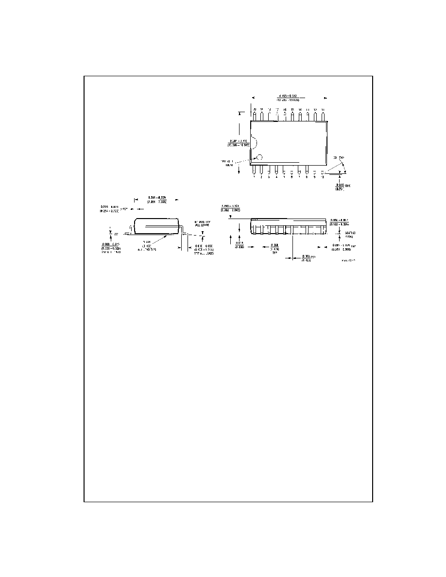
Physical Dimensions
inches (millimeters) unless otherwise noted
20-Lead Small Outline Integrated Circuit (SOIC), JEDEC MS-013, 0.300" Wide
Package Number M20B
5
www.fairchildsemi.com
7
4
VH
C54
1
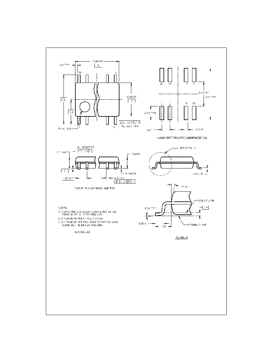
Physical Dimensions
inches (millimeters) unless otherwise noted (Continued)
Pb-Free 20-Lead Small Outline Package (SOP), EIAJ TYPE II, 5.3mm Wide
Package Number M20D