Äîêóìåíòàöèÿ è îïèñàíèÿ www.docs.chipfind.ru
© 2005 Fairchild Semiconductor Corporation
DS011563
www.fairchildsemi.com
March 1993
Revised May 2005
7
4
VH
C57
3
Oct
a
l
D-
T
ype Lat
ch
w
i
t
h
3-
ST
A
T
E
O
u
tput
s
74VHC573
Octal D-Type Latch with 3-STATE Outputs
General Description
The VHC573 is an advanced high speed CMOS octal latch
with 3-STATE output fabricated with silicon gate CMOS
technology. It achieves the high speed operation similar to
equivalent Bipolar Schottky TTL while maintaining the
CMOS low power dissipation. This 8-bit D-type latch is con-
trolled by a latch enable input (LE) and an Output Enable
input (OE). When the OE input is HIGH, the eight outputs
are in a high impedance state.
An input protection circuit ensures that 0V to 7V can be
applied to the input pins without regard to the supply volt-
age. This device can be used to interface 5V to 3V systems
and two supply systems such as battery back up. This cir-
cuit prevents device destruction due to mismatched supply
and input voltages.
Features
s
High Speed: t
PD
5.0 ns (typ) at V
CC
5V
s
High Noise Immunity: V
NIH
V
NIL
28% V
CC
(Min)
s
Power Down Protection is provided on all inputs
s
Low Noise: V
OLP
0.6V (typ)
s
Low Power Dissipation: I
CC
4
P
A (Max) @ T
A
25
q
C
s
Pin and function compatible with 74HC573
Ordering Code:
Surface mount packages are also available on Tape and Reel. Specify by appending the suffix letter "X" to the ordering code.
Pb-Free package per JEDEC J-STD-020B.
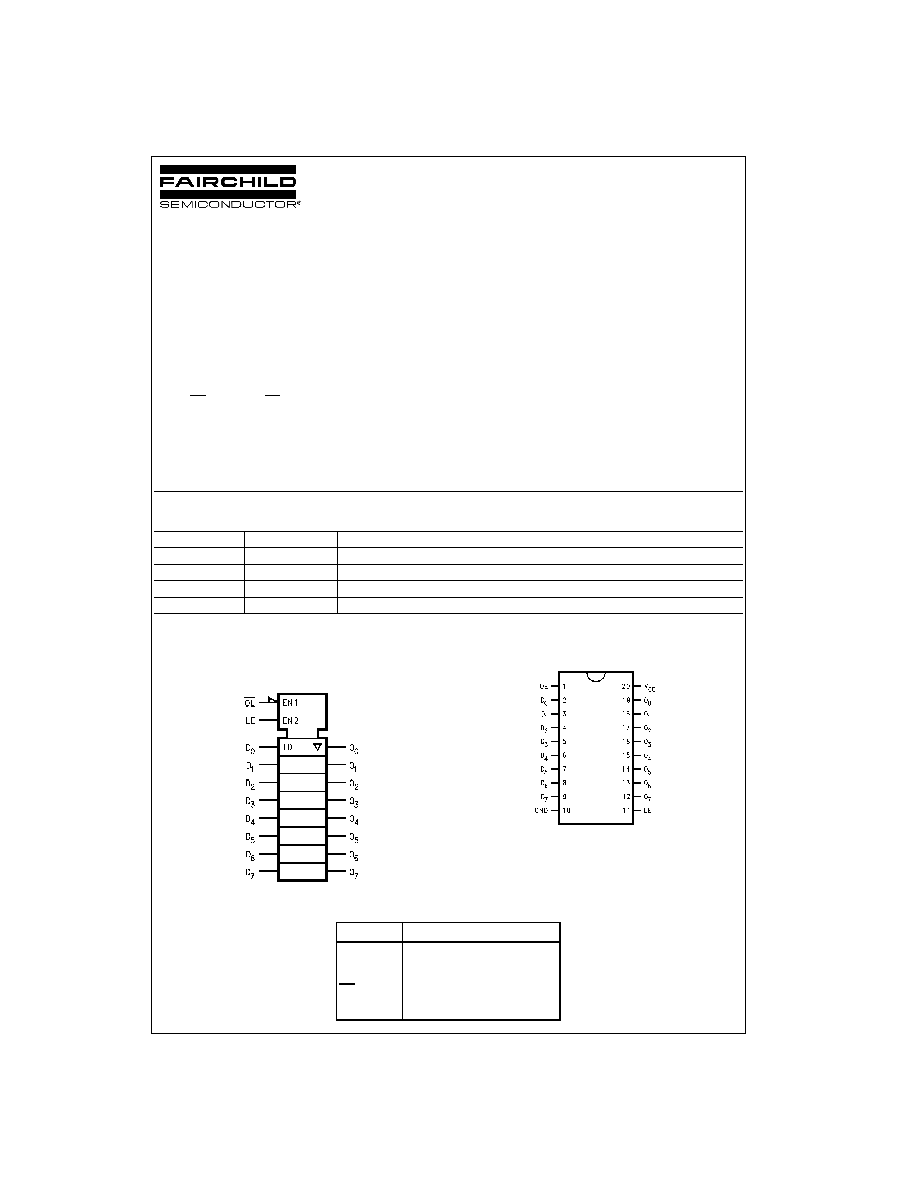
Logic Symbol
IEEE/IEC
Connection Diagram
Pin Descriptions
Order Number
Package Number
Package Description
74VHC573M
M20B
20-Lead Small Outline Integrated Circuit (SOIC), JEDEC MS-013, 0.300" Wide
74VHC573SJ
M20D
Pb-Free 20-Lead Small Outline Package (SOP), EIAJ TYPE II, 5.3mm Wide
74VHC573MTC
MTC20
20-Lead Thin Shrink Small Outline Package (TSSOP), JEDEC MO-153, 4.4mm Wide
74VHC573N
N20A
20-Lead Plastic Dual-In-Line Package (PDIP), JEDEC MS-001, 0.300" Wide
Pin Names
Description
D
0
D
7
Data Inputs
LE
Latch Enable Input
OE
3-STATE Output Enable Input
O
0
O
7
3-STATE Outputs
www.fairchildsemi.com
2
74
V
HC573
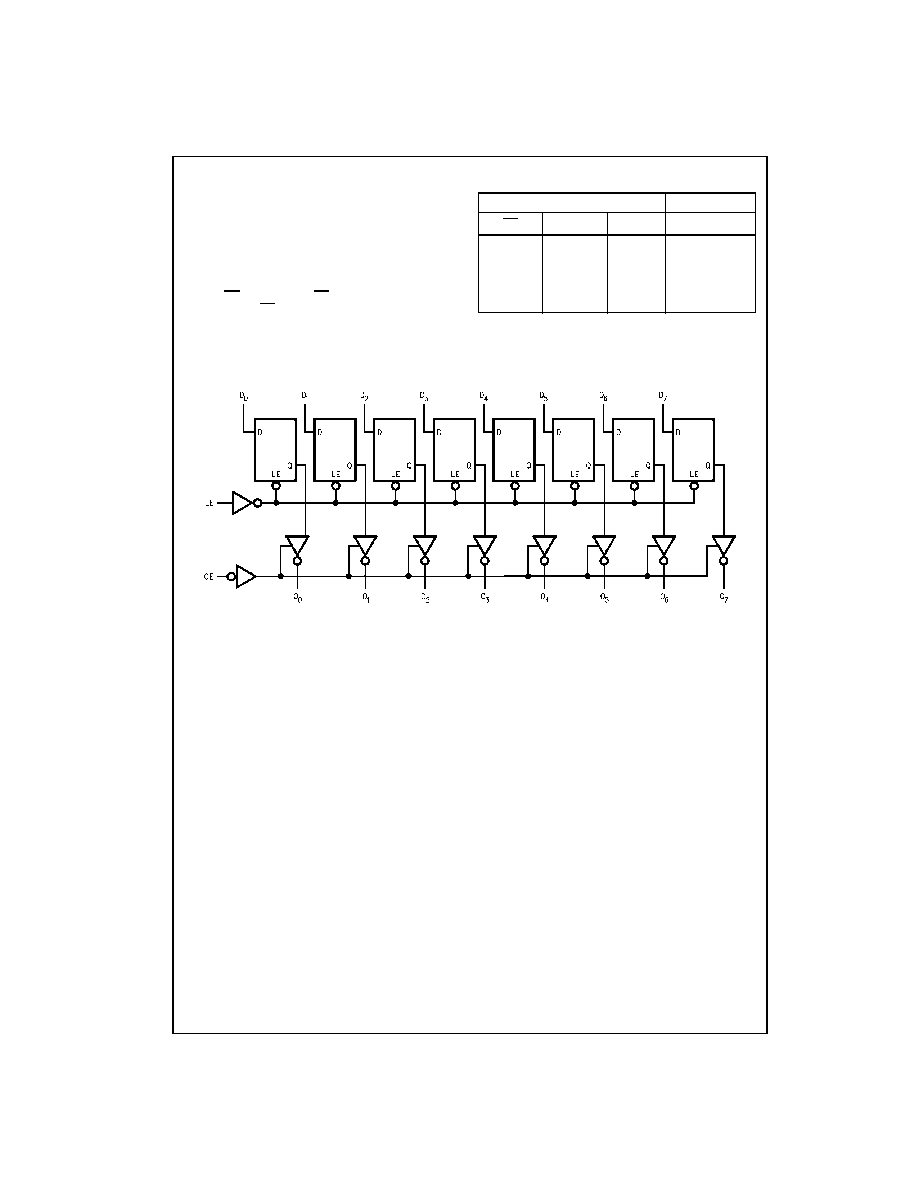
Functional Description
The VHC573 contains eight D-type latches with 3-STATE
output buffers. When the Latch Enable (LE) input is HIGH,
data on the D
n
inputs enters the latches. In this condition
the latches are transparent, i.e., a latch output will change
state each time its D input changes. When LE is LOW the
latches store the information that was present on the D
inputs, a setup time preceding the HIGH-to-LOW transition
of LE. The 3-STATE buffers are controlled by the Output
Enable (OE) input. When OE is LOW, the buffers are
enabled. When OE is HIGH the buffers are in the high
impedance mode, but, this does not interfere with entering
new data into the latches.
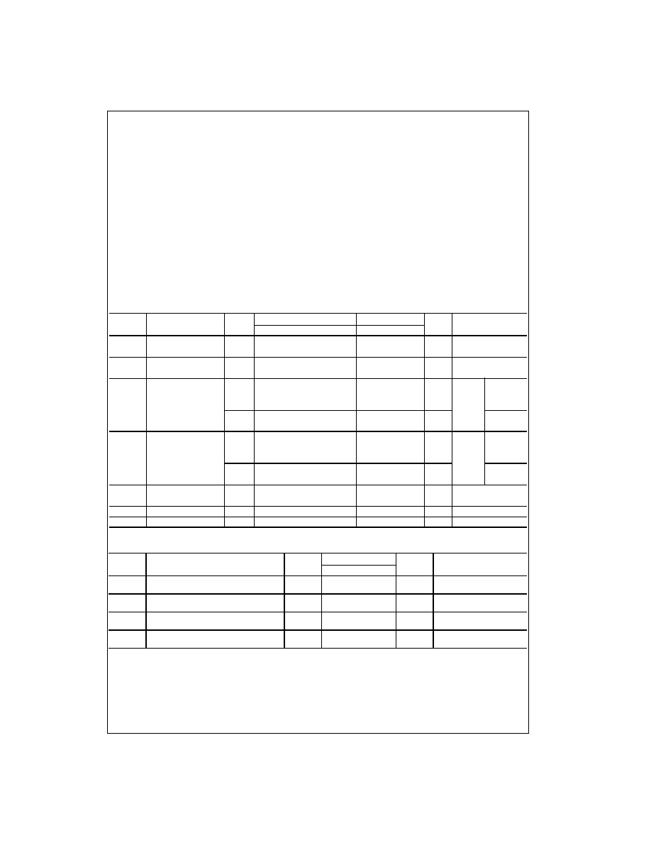
Truth Table
H
HIGH Voltage Level
L
LOW Voltage Level
X
Immaterial
Z
High Impedance
Logic Diagram
Please note that this diagram is provided only for the understanding of logic operations and should not be used to estimate propagation delays.
Inputs
Outputs
OE
LE
D
O
n
L
H
H
H
L
H
L
L
L
L
X
O
0
H
X
X
Z
3
www.fairchildsemi.com
7
4
VH
C57
3
Absolute Maximum Ratings
(Note 1)
Recommended Operating
Conditions
(Note 2)
Note 1: Absolute Maximum Ratings are values beyond which the device
may be damaged or have its useful life impaired. The databook specifica-
tions should be met, without exception, to ensure that the system design is
reliable over its power supply, temperature, and output/input loading vari-
ables. Fairchild does not recommend operation outside databook specifica-
tions.
Note 2: Unused inputs must be held HIGH or LOW They may not float.
DC Electrical Characteristics
Noise Characteristics
Note 3: Parameter guaranteed by design.
Supply Voltage (V
CC
)
0.5V to
7.0V
DC Input Voltage (V
IN
)
0.5V to
7.0V
DC Output Voltage (V
OUT
)
0.5V to V
CC
0.5V
Input Diode Current (I
IK
)
20 mA
Output Diode Current
r
20 mA
DC Output Current (I
OUT
)
r
25 mA
DC V
CC
/GND Current (I
CC
)
r
75 mA
Storage Temperature (T
STG
)
65
q
C to
150
q
C
Lead Temperature (T
L
)
(Soldering, 10 seconds)
260
q
C
Supply Voltage (V
CC
)
2.0V to
5.5V
Input Voltage (V
IN
)
0V to
5.5V
Output Voltage (V
OUT
)
0V to V
CC
Operating Temperature (T
OPR
)
40
q
C to
85
q
C
Input Rise and Fall Time (t
r
, t
f
)
V
CC
3.3V
r
0.3V
0
a
100 ns/V
V
CC
5.0V
r
0.5V
0
a
20 ns/V
Symbol
Parameter
V
CC
(V)
T
A
25
q
C
T
A
40
q
C to
85
q
C
Units
Conditions
Min
Typ
Max
Min
Max
V
IH
HIGH Level Input
2.0
1.50
1.50
V
Voltage
3.0
5.5
0.7 V
CC
0.7 V
CC
V
IL
LOW Level Input
2.0
0.50
0.50
V
Voltage
3.0
5.5
0.3 V
CC
0.3 V
CC
V
OH
HIGH Level Output
2.0
1.9
2.0
1.9
V
V
IN
V
IH
Voltage
3.0
2.9
3.0
2.9
or V
IL
I
OH
50
P
A
4.5
4.4
4.5
4.4
3.0
2.58
2.48
V
I
OH
4 mA
4.5
3.94
3.80
I
OH
8 mA
V
OL
LOW Level Output
2.0
0.0
0.1
0.1
V
V
IN
V
IH
Voltage
3.0
0.0
0.1
0.1
or V
IL
I
OL
50
P
A
4.5
0.0
0.1
0.1
3.0
0.36
0.44
V
I
OL
4 mA
4.5
0.36
0.44
I
OL
8 mA
I
OZ
3-STATE Output
5.5
r
0.25
r
2.5
P
A
V
IN
V
IH
or V
IL
Off-State Current
V
OUT
V
CC
or GND
I
IN
Input Leakage Current
0
5.5
r
0.1
r
1.0
P
A
V
IN
5.5V or GND
I
CC
Quiescent Supply Current
5.5
4.0
40.0
P
A
V
IN
V
CC
or GND
Symbol
Parameter
V
CC
(V)
T
A
25
q
C
Units
Conditions
Typ
Limits
V
OLP
(Note 3)
Quiet Output Maximum Dynamic V
OL
5.0
0.9
1.2
V
C
L
50 pF
V
OLV
(Note 3)
Quiet Output Minimum Dynamic V
OL
5.0
0.8
1.0
V
C
L
50 pF
V
IHD
(Note 3)
Minimum HIGH Level Dynamic Input Voltage
5.0
3.5
V
C
L
50 pF
V
ILD
(Note 3)
Maximum LOW Level Dynamic Input Voltage
5.0
1.5
V
C
L
50 pF
www.fairchildsemi.com
4
74
V
HC573
AC Electrical Characteristics
Note 4: Parameter guaranteed by design. t
OSLH
|t
PLH max
t
PLH min
|; t
OSHL
|t
PHL max
t
PHL min
|
Note 5: C
PD
is defined as the value of the internal equivalent capacitance which is calculated from the operating current consumption without load. Average
operating current can be obtained by the equation: I
CC
(opr.)
C
PD
* V
CC
* f
IN
I
CC
/8 (per Latch). The total C
PD
when n pcs. of the Latch operates can be
calculated by the equation: C
PD
(total)
21
8n.
AC Operating Requirements
Symbol
Parameter
V
CC
(V)
T
A
25
q
C
T
A
40
q
C to
85
q
C
Units
Conditions
Min
Typ
Max
Min
Max
t
PLH
Propagation Delay
3.3
r
0.3
7.6
11.9
1.0
14.0
ns
C
L
15 pF
t
PHL
Time (LE to O
n
)
10.1
15.4
1.0
17.5
C
L
50 pF
5.0
r
0.5
5.0
7.7
1.0
9.0
ns
C
L
15 pF
6.5
9.7
1.0
11.0
C
L
50 pF
t
PLH
Propagation Delay
3.3
r
0.3
7.0
11.0
1.0
13.0
ns
C
L
15 pF
t
PHL
Time (DO
n
)
9.5
14.5
1.0
16.5
C
L
50 pF
5.0
r
0.5
4.5
6.8
1.0
8.0
C
L
15 pF
6.0
8.8
1.0
10.0
C
L
50 pF
t
PZL
3-STATE Output
3.3
r
0.3
7.3
11.5
1.0
13.5
ns
R
L
1 k
:
C
L
15 pF
t
PZH
Enable Time
9.8
15.0
1.0
17.0
C
L
50 pF
5.0
r
0.5
5.2
7.7
1.0
9.0
ns
C
L
15 pF
6.7
9.7
1.0
11.0
C
L
50 pF
t
PLZ
3-STATE Output
3.3
r
0.3
10.7
14.5
1.0
16.5
ns
R
L
1 k
:
C
L
50 pF
t
PHZ
Disable Time
5.0
r
0.5
6.7
9.7
1.0
11.0
C
L
50 pF
t
OSLH
Output to Output Skew
3.3
r
0.3
1.5
1.5
ns
(Note 4)
C
L
50 pF
t
OSHL
5.0
r
0.5
1.0
1.0
C
L
50 pF
C
IN
Input Capacitance
4
10
10
pF
V
CC
Open
C
OUT
Output Capacitance
6
pF
V
CC
5.0V
C
PD
Power Dissipation
29
pF
(Note 5)
Capacitance
Symbol
Parameter
V
CC
(V)
T
A
25
q
C
T
A
40
q
C to
85
q
C
Units
Min
Typ
Max
Min
Max
t
w
(H)
Minimum Pulse
3.3
r
0.3
5.0
5.0
ns
t
w
(L)
Width (LE)
5.0
r
0.5
5.0
5.0
t
S
Minimum Setup Time
3.3
r
0.3
3.5
3.5
ns
5.0
r
0.5
3.5
3.5
t
H
Minimum Hold Time
3.3
r
0.3
1.5
1.5
ns
5.0
r
0.5
1.5
1.5
5
www.fairchildsemi.com
7
4
VH
C57
3
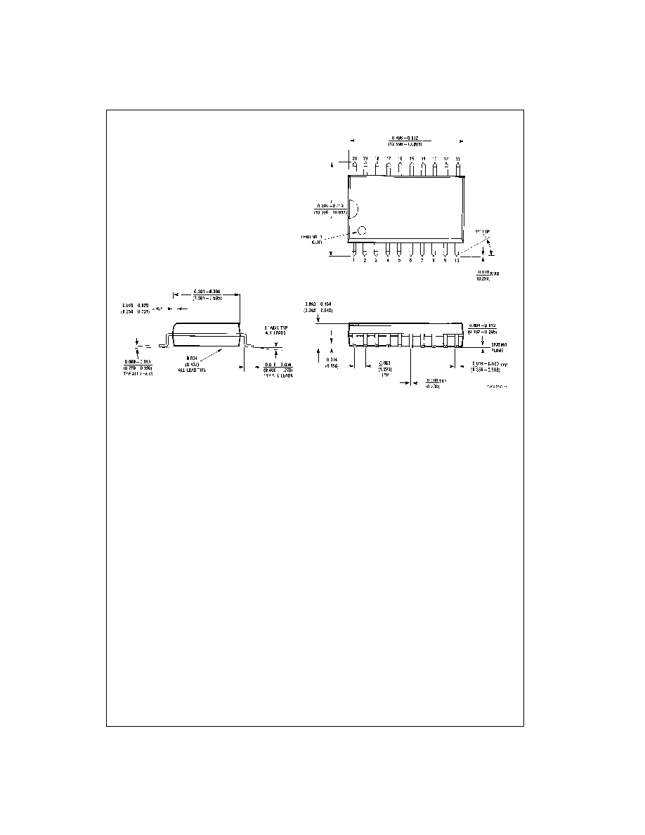
Physical Dimensions
inches (millimeters) unless otherwise noted
20-Lead Small Outline Integrated Circuit (SOIC), JEDEC MS-013, 0.300" Wide
Package Number M20B