© 2005 Fairchild Semiconductor Corporation
DS500004
www.fairchildsemi.com
March 1997
Revised April 2005
7
4
VH
CT2
45A
Oct
a
l
Buf
f
er
/Li
ne D
r
ive
r
w
i
th 3-
S
T
A
T
E O
u
t
put
s
74VHCT245A
Octal Buffer/Line Driver with 3-STATE Outputs
General Description
The VHCT245A is an advanced high speed CMOS octal
bus transceiver fabricated with silicon gate CMOS technol-
ogy. It achieves high speed operation similar to equivalent
Bipolar Schottky TTL while maintaining the CMOS low
power dissipation. The VHCT245A is intended for bidirec-
tional asynchronous communication between data busses.
The direction of data transmission is determined by the
level of the T/R input. The enable input can be used to dis-
able the device so that the busses are effectively isolated.
Protection circuits ensure that 0V to 7V can be applied to
the input and output (Note 1) pins without regard to the
supply voltage. These circuits prevent device destruction
due to mismatched supply and input/output voltages. This
device can be used to interface 5V to 3V systems and two
supply systems such as battery back up.
Note 1: Outputs in OFF-State
Features
s
High Speed:
t
PD
5.4 ns (typ) at V
CC
5V
s
Power Down Protection on Inputs and Outputs
s
Low Power Dissipation:
I
CC
4
P
A (Max) @ T
A
25
q
C
s
Pin and Function Compatible with 74HCT245
Ordering Code:
Surface mount packages are also available on Tape and Reel. Specify by appending the suffix letter "X" to the ordering code.
Pb-Free package per JEDED J-STD-020B.
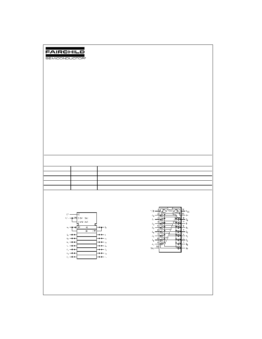
Logic Symbol
IEEE/IEC
Connection Diagram
Order Number
Package Number
Package Description
74VHCT245AM
M20B
20-Lead Small Outline Integrated Circuit (SOIC), JEDEC MS-013, 0.300" Wide
74VHCT245ASJ
M20D
Pb-Free 20-Lead Small Outline Package (SOP), EIAJ TYPE II, 5.3mm Wide
74VHCT245AMTC
MTC20
20-Lead Thin Shrink Small Outline Package (TSSOP), JEDEC MO-153, 4.4mm Wide
74VHCT245AN
N20A
20-Lead Plastic Dual-In-Line Package (PDIP), JEDEC MS-001, 0.300" Wide

www.fairchildsemi.com
2
7
4
VH
CT24
5A
Pin Descriptions
Truth Table
H
HIGH Voltage Level
L
LOW Voltage Level
X
Immaterial
Pin Names
Description
OE
Output Enable Input
T/R
Transmit/Receive Input
A
0
≠A
7
Side A Inputs or 3-STATE Outputs
B
0
≠B
7
Side B Inputs or 3-STATE Outputs
Inputs
Outputs
OE
T/R
L
L
Bus B Data to Bus A
L
H
Bus A Data to Bus B
H
X
HIGH-Z State
3
www.fairchildsemi.com
7
4
VH
CT2
45A
Absolute Maximum Ratings
(Note 2)
Recommended Operating
Conditions
(Note 6)
Note 2: Absolute Maximum Ratings are values beyond which the device
may be damaged or have its useful life impaired. The databook specifica-
tions should be met, without exception, to ensure that the system design is
reliable over its power supply, temperature, and output/input loading vari-
ables. Fairchild does not recommend operation outside databook specifica-
tions.
Note 3: HIGH or LOW state. I
OUT
absolute maximum rating must be
observed.
Note 4: When outputs are in OFF-State or when V
CC
OV.
Note 5: V
OUT
GND, V
OUT
!
V
CC
(Outputs Active).
Note 6: Unused inputs must be held HIGH or LOW. They may not float.
DC Electrical Characteristics
Supply Voltage (V
CC
)
0.5V to
7.0V
DC Input Voltage (V
IN
)
0.5V to
7.0V
DC Output Voltage (V
OUT
)
(Note
3)
0.5V to V
CC
0.5V
(Note
4)
0.5V to
7.0V
Input Diode Current (I
IK
)
20 mA
Output Diode Current (I
OK
) (Note 5)
r
20 mA
DC Output Current (I
OUT
)
r
25 mA
DC V
CC
/GND Current (I
CC
)
r
75 mA
Storage Temperature (T
STG
)
65
q
C to
150
q
C
Lead Temperature (T
L
)
(Soldering, 10 seconds)
260
q
C
Supply Voltage (V
CC
)
4.5V to
5.5V
Input Voltage (V
IN
)
0V to
5.5V
Output Voltage (V
OUT
)
(Note 3)
0V to V
CC
(Note 4)
0V to
5.5V
Operating Temperature (T
OPR
)
40
q
C to
85
q
C
Input Rise and Fall Time (t
r
, t
f
)
V
CC
5.0V
r
0.5V
0 ns/V
a
20 ns/V
Symbol
Parameter
V
CC
T
A
25
q
C
T
A
40
q
C to
85
q
C
Units
Conditions
(V)
Min
Typ
Max
Min
Max
V
IH
HIGH Level
4.5
2.0
2.0
V
Input Voltage
5.5
2.0
2.0
V
IL
LOW Level
4.5
0.8
0.8
V
Input Voltage
5.5
0.8
0.8
V
OH
HIGH Level
4.5
4.40
4.50
4.40
V
V
IN
V
IH
I
OH
50
P
A
Output Voltage
3.94
3.80
V
or V
IL
I
OH
8 mA
V
OL
LOW Level
4.5
0.0
0.1
0.1
V
V
IN
V
IH
I
OL
50
P
A
Output Voltage
0.36
0.44
V
or V
IL
I
OL
8
mA
I
OZ
3-STATE Output
5.5
r
0.25
r
2.5
P
A
V
IN
V
IH
or V
IL
Off-State Current
V
OUT
V
CC
or GND
I
IN
Input Leakage
0≠5.5
r
0.1
r
1.0
P
A
V
IN
5.5V or GND
Current
I
CC
Quiescent Supply
5.5
4.0
40.0
P
A
V
IN
V
CC
or GND
Current
I
CCT
Maximum I
CC
/Input
5.5
1.35
1.50
mA
V
IN
3.4V
Other Input
V
CC
or GND
I
OFF
Output Leakage Current
0.0
0.5
5.0
P
A
V
OUT
5.5V
(Power Down State)
www.fairchildsemi.com
4
7
4
VH
CT24
5A
Noise Characteristics
Note 7: Parameter guaranteed by design.
AC Electrical Characteristics
Note 8: Parameter guaranteed by design. t
OSLH
|t
PLH max
t
PLH min
|; t
OSHL
|t
PHL max
t
PHL min
|
Note 9: C
PD
is defined as the value of the internal equivalent capacitance which is calculated from the operating current consumption without load. Average
operating current can be obtained by the equation: I
CC
(opr.)
C
PD
* V
CC
* f
IN
I
CC
/8 (per F/F). The total C
PD
when n pcs. of the Octal D Flip-Flop operates
can be calculated by the equation: C
PD
(total)
20
12n.
Symbol
Parameter
V
CC
T
A
25
q
C
Units
Conditions
(V)
Typ
Limits
V
OLP
(Note 7)
Quiet Output Maximum Dynamic V
OL
5.0
1.2
1.6
V
C
L
50 pF
V
OLV
(Note 7)
Quiet Output Minimum Dynamic V
OL
5.0
1.2
1.6
V
C
L
50 pF
V
IHD
(Note 7)
Minimum HIGH Level Dynamic Input Voltage
5.0
2.0
V
C
L
50 pF
V
ILD
(Note 7)
Maximum LOW Level Dynamic Input Voltage
5.0
0.8
V
C
L
50 pF
Symbol
Parameter
V
CC
T
A
25
q
C
T
A
40
q
C to
85
q
C
Units
Conditions
(V)
Min
Typ
Max
Min
Max
t
PLH
Propagation Delay
5.0
r
0.5
4.9
7.7
1.0
8.5
ns
C
L
15 pF
t
PHL
Time
5.4
8.7
1.0
9.5
C
L
50 pF
t
PZL
3-STATE Output
5.0
r
0.5
9.4
13.8
1.0
15.0
ns
R
L
1 k
:
C
L
15 pF
t
PZH
Enable Time
9.9
14.8
1.0
16.0
C
L
50 pF
t
PLZ
3-STATE Output
5.0
r
0.5
10.1
15.4
1.0
16.5
ns
R
L
1 k
:
C
L
50 pF
t
PHZ
Disable Time
t
OSLH
Output to
5.0
r
0.5
1.0
1.0
ns
(Note 8)
t
OSHL
Output Skew
C
IN
Input
4
10
10
pF
V
CC
Open
Capacitance
C
OUT
Output
13
pF
V
CC
5.0V
Capacitance
C
PD
Power Dissipation
16
pF
(Note 9)
Capacitance
5
www.fairchildsemi.com
7
4
VH
CT2
45A
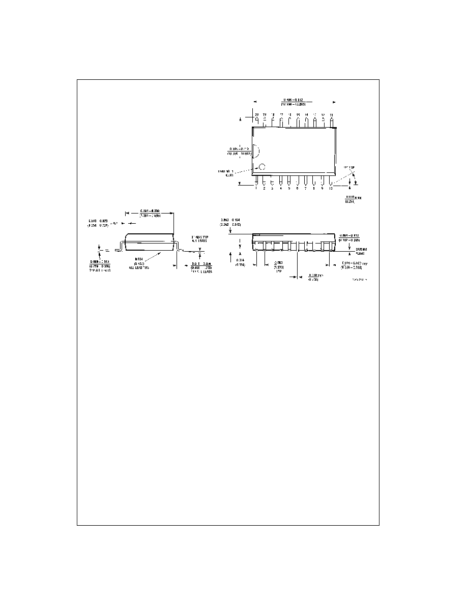
Physical Dimensions
inches (millimeters) unless otherwise noted
20-Lead Small Outline Integrated Circuit (SOIC), JEDEC MS-013, 0.300" Wide
Package Number M20B