© 2005 Fairchild Semiconductor Corporation
DS500026
www.fairchildsemi.com
July 1997
Revised February 2005
7
4
VH
CT7
4
A
Dual
D-
T
y
pe Fl
ip-
F
l
op wi
th
Preset
and
Cl
ear
74VHCT74A
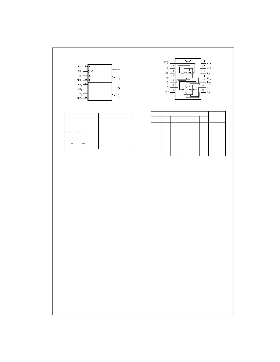
Dual D-Type Flip-Flop with Preset and Clear
General Description
The VHCT74A is an advanced high speed CMOS Dual
D-Type Flip-Flop fabricated with silicon gate CMOS tech-
nology. It achieves the high speed operation similar to
equivalent Bipolar Schottky TTL while maintaining the
CMOS low power dissipation. The signal level applied to
the D INPUT is transferred to the Q OUTPUT during the
positive going transition of the CK pulse. CLR and PR are
independent of the CK and are accomplished by setting the
appropriate input LOW.
Protection circuits ensure that 0V to 7V can be applied to
the input pins without regard to the supply voltage and to
the output pins with V
CC
0V. These circuits prevent
device destruction due to mismatched supply and input/
output voltages. This device can be used to interface 3V to
5V systems and two supply systems such as battery
backup.
Features
s
High speed: f
MAX
160 MHz (typ) at T
A
25
q
C
s
High noise immunity: V
IH
2.0V, V
IL
0.8V
s
Power down protection is provided on all inputs and
outputs
s
Low power dissipation:
I
CC
2
P
A (max) at T
A
25
q
C
s
Pin and function compatible with 74HCT74
Ordering Code:
Surface mount packages are also available on Tape and Reel. Specify by appending the suffix letter "X" to the ordering code.
Pb-Free package per JEDEC J-STD-020B.
Note 1: "_NL" indicates Pb-Free package (per JEDEC J-STD-020B). Device available in Tape and Reel only.
Order Number
Package
Package Description
Number
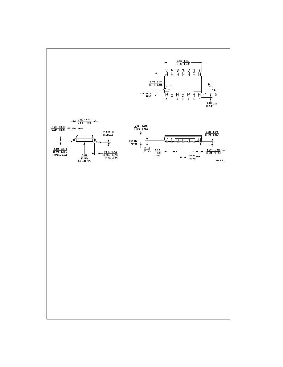
74VHCT74AM
M14A
14-Lead Small Outline Integrated Circuit (SOIC), JEDEC MS-012, 0.150" Narrow
74VHCT74AMX_NL
(Note 1)
M14A
Pb-Free 14-Lead Small Outline Integrated Circuit (SOIC), JEDEC MS-012, 0.150" Narrow
74VHCT74ASJ
M14D
Pb-Free 14-Lead Small Outline Package (SOP), EIAJ TYPE II, 5.3mm Wide
74VHCT74AMTC
MTC14
14-Lead Thin Shrink Small Outline Package (TSSOP), JEDEC MO-153, 4.4mm Wide
74VHCT74AMTCX_NL
(Note 1)
MTC14
Pb-Free 14-Lead Thin Shrink Small Outline Package (TSSOP), JEDEC MO-153, 4.4mm
Wide
74VHCT74AN
N14A
14-Lead Plastic Dual-In-Line Package (PDIP), JEDEC MS-001, 0.300" Wide

3
www.fairchildsemi.com
7
4
VH
CT7
4
A
Absolute Maximum Ratings
(Note 2)
Recommended Operating
Conditions
(Note 6)
Note 2: Absolute maximum ratings are values beyond which the device
may be damaged or have its useful life impaired. The databook specifica-
tions should be met, without exception, to ensure that the system design is
reliable over its power supply, temperature, and output/input loading varai-
bles. Fairchild does not recommend operation outside databook specifica-
tions.
Note 3: HIGH or LOW state. I
OUT
absolute maximum rating must be
observed.
Note 4: V
CC
0V.
Note 5: V
OUT
GND, V
OUT
!
V
CC
.(Outputs Active)
Note 6: Unused inputs must be held HIGH or LOW. They may not float.
DC Electrical Characteristics
Supply Voltage (V
CC
)
0.5V to
7.0V
DC Input Voltage (V
IN
)
0.5V to
7.0V
DC Output Voltage (V
OUT
)
(Note 3)
0.5V to V
CC
0.5V
(Note 4)
0.5V to 7.0V
Input Diode Current (I
IK
)
20 mA
Output Diode Current (I
OK
)
(Note 5)
r
20 mA
DC Output Current (I
OUT
)
r
25 mA
DC V
CC
/GND Current (I
CC
)
r
50 mA
Storage Temperature (T
STG
)
65
q
C to
150
q
C
Lead Temperature (T
L
)
Soldering (10 seconds)
260
q
C
Supply Voltage (V
CC
)
4.5V to 5.5V
Input Voltage (V
IN
)
0V to
5.5V
Output Voltage (V
OUT
)
(Note 3)
0V to V
CC
(Note 4)
0V to 5.5V
Operating Temperature (T
OPR
)
40
q
C to
85
q
C
Input Rise and Fall Time (t
r
, t
f
)
V
CC
5.0V
r
0.5V
0 ns/V
a
20 ns/V
Symbol
Parameter
V
CC
T
A
25
q
C
T
A
40
q
C to
85
q
C
Units
Conditions
(V)
Min
Typ
Max
Min
Max
V
IH
HIGH Level
4.5
2.0
2.0
V
Input Voltage
5.5
2.0
2.0
V
IL
LOW Level
4.5
0.8
0.8
V
Input Voltage
5.5
0.8
0.8
V
OH
HIGH Level
4.5
4.40
4.50
4.40
V
V
IN
V
IH
I
OH
50
P
A
Output Voltage
4.5
3.94
3.80
or V
IL
I
OH
8 mA
V
OL
LOW Level
4.5
0.0
0.1
0.1
V
V
IN
V
IH
I
OL
50
P
A
Output Voltage
4.5
0.36
0.44
or V
IL
I
OL
8 mA
I
IN
Input Leakage Current
0≠5.5
r
0.1
r
1.0
P
A
V
IN
5.5V or GND
I
CC
Quiescent Supply Current
5.5
2.0
20.0
P
A
V
IN
V
CC
or GND
I
CCT
Maximum I
CC
/Input
5.5
1.35
1.50
mA
V
IN
3.4V
Other Inputs
V
CC
or GND
I
OFF
Output Leakage Current
0.0
0.5
5.0
P
A
V
OUT
5.5V
(Power Down State)
www.fairchildsemi.com
4
74VHC
T7
4A
AC Electrical Characteristics
Note 7: V
CC
is 5.0
r
0.5V
Note 8: C
PD
is defined as the value of internal equivalent capacitance which is calculated from the operating current consumption without load. Average
operating current can be obtained by the equation: I
CC
(opr)
C
PD
u
V
CC
u
f
IN
I
CC
/2 (per flip-flop).
AC Operating Requirements
Symbol
Parameter
V
CC
(V)
(Note 7)
T
A
25
q
C
T
A
40
q
C to
85
q
C
Units
Conditions
Min
Typ
Max
Min
Max
f
MAX
Maximum Clock
5.0
100
160
80
MHz
C
L
15 pF
Frequency
5.0
80
140
65
C
L
50 pF
t
PLH
Propagation Delay Time
5.0
5.8
7.8
1.0
9.0
ns
C
L
15 pF
t
PHL
(CK-Q, Q)
5.0
6.3
8.8
1.0
10.0
C
L
50 pF
t
PLH
Propagation Delay time
5.0
7.6
10.4
1.0
12.0
ns
C
L
15 pF
t
PHL
(CLR, PR -Q, Q)
5.0
8.1
11.4
1.0
13.0
C
L
50 pF
C
IN
Input Capacitance
4
10
10
pF
V
CC
Open
C
PD
Power Dissipation Capacitance
24
pF
(Note 8)
Symbol
Parameter
V
CC
T
A
25
q
C
T
A
40
q
C to
85
q
C
Units
(V)
Typ
Guaranteed Minimum
t
W
(L)
Minimum Pulse Width (CK)
5.0
r
0.5
5.0
5.0
ns
t
W
(H)
t
W
(L)
Minimum Pulse Width
5.0
r
0.5
5.0
5.0
ns
(CLR, PR)
t
S
Minimum Setup Time
5.0
r
0.5
5.0
5.0
ns
t
H
Minimum Hold Time
5.0
r
0.5
0
0
ns
t
REM
Minimum Removal Time
5.0
r
0.5
3.5
3.5
ns
(CLR, PR)