 | –≠–ª–µ–∫—Ç—Ä–æ–Ω–Ω—ã–π –∫–æ–º–ø–æ–Ω–µ–Ω—Ç: 9368 | –°–∫–∞—á–∞—Ç—å:  PDF PDF  ZIP ZIP |

© 2000 Fairchild Semiconductor Corporation
DS009796
www.fairchildsemi.com
October 1988
Revised March 2000
DM9368
7-
Segm
ent
Dec
oder/
D
ri
ver/
Latch
wit
h
Cons
tant
Cur
r
ent
Sour
ce Out
puts
DM9368
7-Segment Decoder/Driver/Latch
with Constant Current Source Outputs
General Description
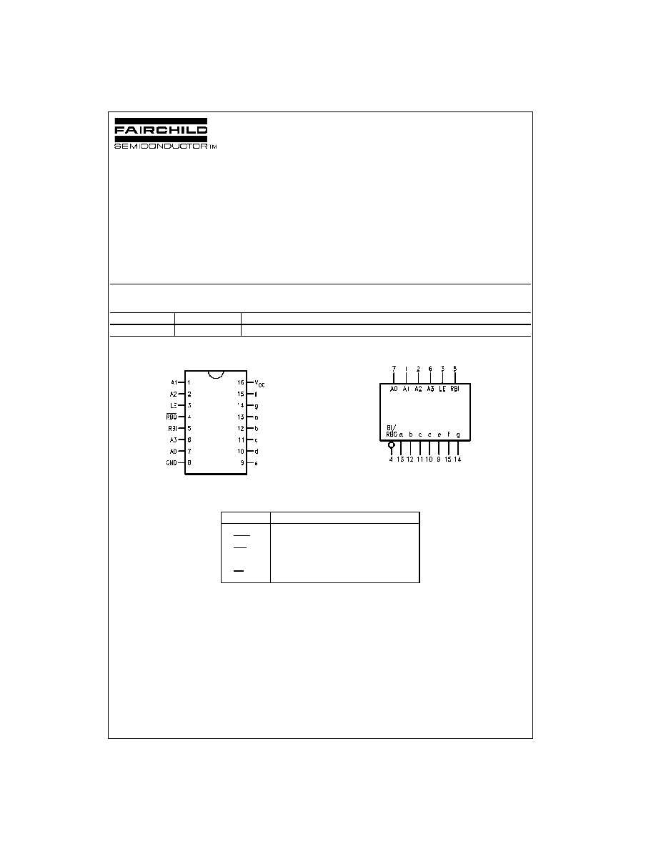
The DM9368 is a 7-segment decoder driver incorporating
input latches and constant current output circuits to drive
common cathode type LED displays directly.
Ordering Code:
Connection Diagram
Logic Symbol
V
CC
=
Pin 16
GND
=
PIN 8
Pin Descriptions
Order Number
Package Number
Package Description
DM9638N
N16E
16-Lead Plastic Dual-In-Line Package (PDIP), JEDEC MS-001, 0.300 Wide
Pin Name
Description
A0≠A3
Address (Data) Inputs
RBO
Ripple Blanking Output (Active LOW)
RBI
Ripple Blanking Input (Active LOW)
a≠g
Segment Drivers-Outputs
LE
Latch Enable Input (Active LOW)

www.fairchildsemi.com
2
D
M
9368
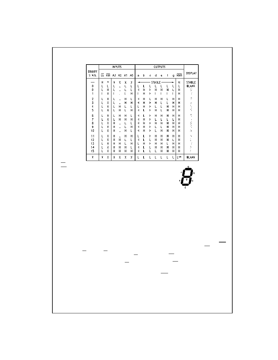
Truth Table
*The RBI will blank the display only if a binary zero is stored in the latches.
*The RBO used as an input overrides all other input conditions.
H
=
HIGH Voltage Level
L
=
LOW Voltage Level
X
=
Immaterial
Functional Description
The DM9368 is a 7-segment decoder driver designed to
drive 7-segment common cathode LED displays. The
DM9368 drives any common cathode LED display rated at
a nominal 20 mA at 1.7V per segment without need for cur-
rent limiting resistors.
This device accepts a 4-bit binary code and produces out-
put drive to the appropriate segments of the 7-segment dis-
play. It has a hexadecimal decode format which produces
numeric codes "0" thru "9" and alpha codes "A" through "F"
using upper and lower case fonts.
Latches on the four data inputs are controlled by an active
LOW latch enable LE. When the LE is LOW, the state of
the outputs is determined by the input data. When the LE
goes HIGH, the last data present at the inputs is stored in
the latches and the outputs remain stable. The LE pulse
width necessary to accept and store data is typically 30 ns
which allows data to be strobed into the DM9368 at normal
TTL speeds. This feature means that data can be routed
directly from high speed counters and frequency dividers
into the display without slowing down the system clock or
providing intermediate data storage.
Another feature of the DM9368 is that the unit loading on
the data inputs is very low (
-
100
µ
A Max) when the latch
enable is HIGH. This allows DM9368s to be driven from an
MOS device in multiplex mode without the need for drivers
on the data lines.
The DM9368 also has provision for automatic blanking of
the leading and/or trailing edge zeros in a multidigit decimal
number, resulting in an easily readable decimal display
conforming to normal writing practice. In an eight digit
mixed integer fraction decimal representation, using the
automatic blanking capability, 0060.0300 would be dis-
played as 60.03. Leading edge zero suppression is
obtained by connecting the Ripple Blanking Output (RBO)
of a decoder to the Ripple Blanking Input (RBI) of the next
lower stage device. The most significant decoder stage
should have the RBI input grounded; and since suppres-
sion of the least significant integer zero in a number is not
usually desired, the RBI input of this decoder stage should
be left open. A similar procedure for the fractional part of a
display will provide automatic suppression of trailing edge
zeros. The RBO terminal of the decoder can be OR-tied
with a modulating signal via an isolating buffer to achieve
pulse duration intensity modulation. A suitable signal can
be generated for this purpose by forming a variable fre-
quency multivibrator with a cross coupled pair of TTL or
DTL gates.

3
www.fairchildsemi.com
DM9368
Logic Diagram
Numerical Designations
Parallel Data Display System with Ripply Blanking
Common Cathode LED Display

www.fairchildsemi.com
4
D
M
9368
Display Demultiplexing System with Ripple Blanking
Common Cathode LED Display
Note: Digit address data must be non-overlapping. Standard TTL decoders like the 9301, 9311, 7442 or 74155 must be strobed, since the address decoding
glitches could cause erroneous data to be strobed into the latches.

5
www.fairchildsemi.com
DM9368
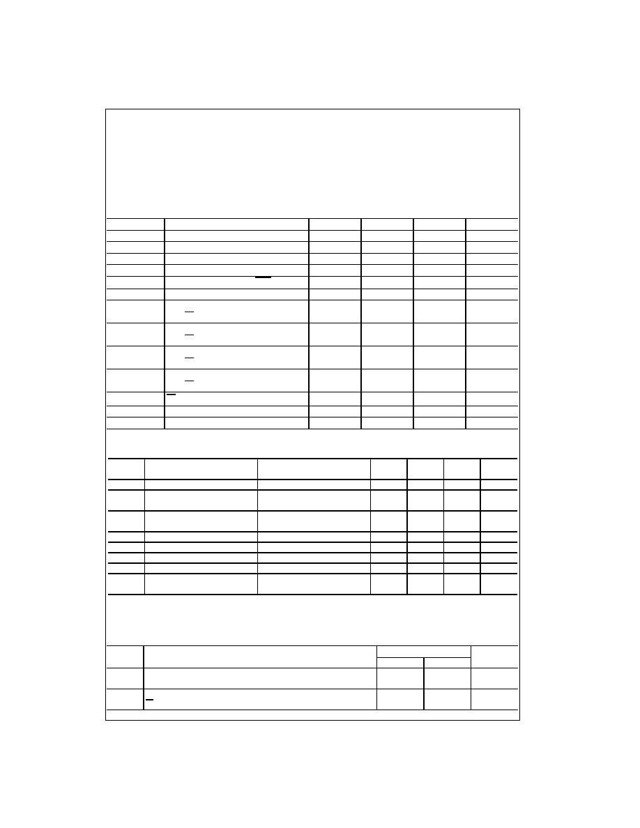
Absolute Maximum Ratings
(Note 1)
Note 1: The "Absolute Maximum Ratings" are those values beyond which
the safety of the device cannot be guaranteed. The device should not be
operated at these limits. The parametric values defined in the Electrical
Characteristics tables are not guaranteed at the absolute maximum ratings.
The "Recommended Operating Conditions" table will define the conditions
for actual device operation.
Recommended Operating Conditions
Electrical Characteristics
Over recommended operating free air temperature range (unless otherwise noted)
Note 2: All typicals are at V
CC
=
5V, T
A
=
25
∞
C.
Note 3: Not more than one output should be shorted at a time.
Switching Characteristics
V
CC
=
5.0V, T
A
=
25
∞
C
Supply Voltage
7V
Input Voltage
5.5V
Operating Free Air Temperature Range
0
∞
C to
+
70
∞
C
Storage Temperature Range
-
65
∞
C to
+
150
∞
C
Symbol
Parameter
Min
Nom
Max
Units
V
CC
Supply Voltage
4.75
5
5.25
V
V
IH
HIGH Level Input Voltage
2
V
V
IL
LOW Level Input Voltage
0.8
V
I
OH
HIGH Level Output Current
-
80
µ
A
I
OL
LOW Level Output Current RBO
3.2
mA
T
A
Free Air Operating Temperature
0
70
∞
C
t
S
(H)
Setup Time HIGH
30
ns
A
n
to LE
t
H
(H)
Hold Time HIGH
0
ns
A
n
to LE
t
S
(L)
Setup Time LOW
20
ns
A
n
to LE
t
H
(L)
Hold Time LOW
0
ns
A
n
to LE
t
W
(L)
LE Pulse Width LOW
45
ns
I
OH
Segment Output HIGH Current
-
16
-
22
mA
I
OL
Segment Output LOW Current
-
250
250
µ
A
Symbol
Parameter
Conditions
Min
Typ
Max
Units
(Note 2)
V
I
Input Clamp Voltage
V
CC
=
Min, I
I
=
-
12 mA
-
1.5
V
V
OH
HIGH Level
V
CC
=
Min, I
OH
=
Max,
2.4
3.4
V
Output Voltage
V
IL
=
Max
V
OL
LOW Level
V
CC
=
Min, I
OL
=
Max,
0.2
0.4
V
Output Voltage
V
IH
=
Min
I
I
Input Current @ Max Input Voltage
V
CC
=
Max, V
I
=
5.5V
1
mA
I
IH
HIGH Level Input Current
V
CC
=
Max, V
I
=
2.4V
40
µ
A
I
IL
LOW Level Input Current
V
CC
=
Max, V
I
=
0.4V
-
1.6
mA
I
OS
Short Circuit Output Current
V
CC
=
Max (Note 3)
-
18
-
57
mA
I
CC
Supply Current
V
CC
=
Max, Outputs OPEN,
67
mA
Data & Latch Inputs
=
0V
Symbol
Parameter
C
L
=
15 pF, R
L
=
100
Units
Min
Max
t
PLH
Propagation Delay
50
ns
t
PHL
A
n
to a≠g
75
t
PLH
Propagation Delay
70
ns
t
PHL
LE to a≠g
90

www.fairchildsemi.com
6
D
M
9368
7-
Segm
en
t
D
e
coder/
D
ri
ver/
Latc
h
wit
h
C
o
nstant
Cur
r
ent
Sour
ce
O
u
t
puts
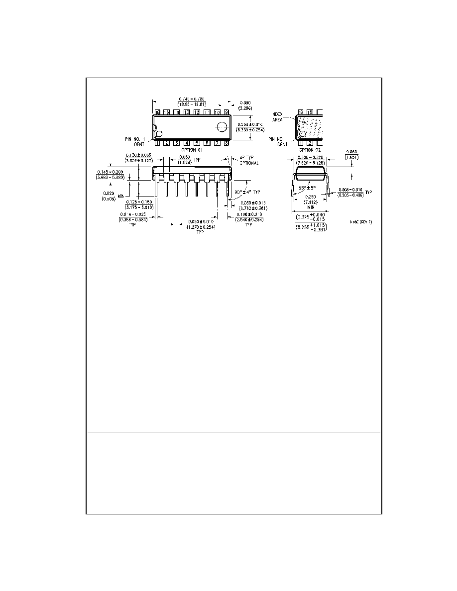
Physical Dimensions
inches (millimeters) unless otherwise noted
16-Lead Plastic Dual-In-Line Package (PDIP), JEDEC MS-001, 0.300 Wide
Package Number N16E
Fairchild does not assume any responsibility for use of any circuitry described, no circuit patent licenses are implied and
Fairchild reserves the right at any time without notice to change said circuitry and specifications.
LIFE SUPPORT POLICY
FAIRCHILD'S PRODUCTS ARE NOT AUTHORIZED FOR USE AS CRITICAL COMPONENTS IN LIFE SUPPORT
DEVICES OR SYSTEMS WITHOUT THE EXPRESS WRITTEN APPROVAL OF THE PRESIDENT OF FAIRCHILD
SEMICONDUCTOR CORPORATION. As used herein:
1. Life support devices or systems are devices or systems
which, (a) are intended for surgical implant into the
body, or (b) support or sustain life, and (c) whose failure
to perform when properly used in accordance with
instructions for use provided in the labeling, can be rea-
sonably expected to result in a significant injury to the
user.
2. A critical component in any component of a life support
device or system whose failure to perform can be rea-
sonably expected to cause the failure of the life support
device or system, or to affect its safety or effectiveness.
www.fairchildsemi.com
