 | –≠–ª–µ–∫—Ç—Ä–æ–Ω–Ω—ã–π –∫–æ–º–ø–æ–Ω–µ–Ω—Ç: 96LS02 | –°–∫–∞—á–∞—Ç—å:  PDF PDF  ZIP ZIP |
© 2000 Fairchild Semiconductor Corporation
DS009816
www.fairchildsemi.com
October 1988
Revised March 2000
DM96LS02 Dual
Ret
r
i
ggerabl
e
Res
e
tt
able Monost
able Mult
ivi
b
rat
o
r
DM96LS02
Dual Retriggerable Resettable Monostable Multivibrator
General Description
The DM96LS02 is a dual retriggerable and resettable
monostable multivibrator. The one-shot provides excep-
tionally wide delay range, pulse width stability, predictable
accuracy and immunity to noise. The pulse width is set by
an external resistor and capacitor. Resistor values up to 1.0
M
reduce required capacitor values. Hysteresis is pro-
vided on both trigger inputs of the DM96LS02 for increased
noise immunity.
Features
s
Required timing capacitance reduced by factors of 10 to
100 over conventional designs
s
Broad timing resistor range--1.0 k
to 2.0 M
s
Output Pulse Width is variable over a 2000:1 range by
resistor control
s
Propagation delay of 35 ns
s
0.3V hysteresis on trigger inputs
s
Output pulse width independent of duty cycle
s
35 ns to
output pulse width range
Ordering Code:
Devices also available in Tape and Reel. Specify by appending the suffix letter "X" to the ordering code.
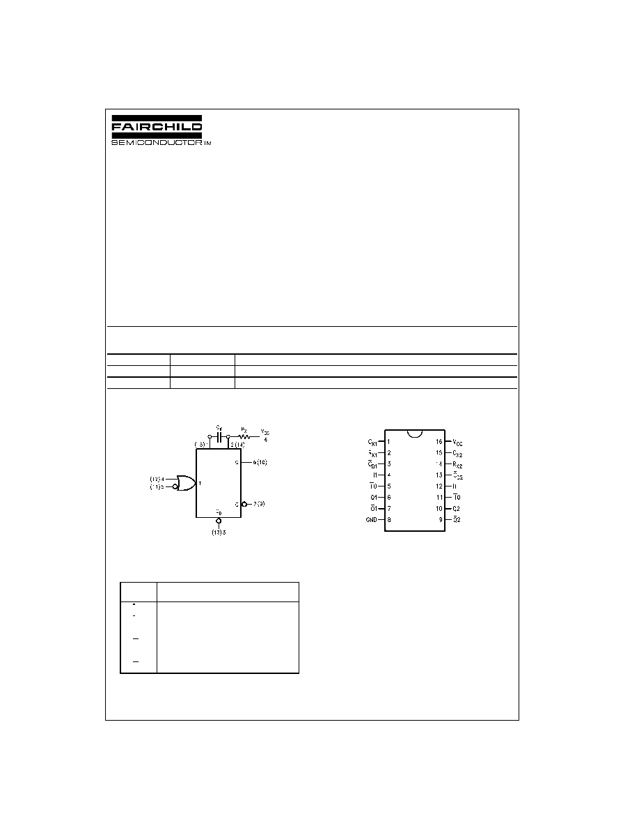
Logic Symbol
V
CC
=
Pin 16
GND
=
Pin 8
Pin Descriptions
Connection Diagram
Order Number
Package Number
Package Description
DM96LS02M
M16A
16-Lead Small Outline Integrated Circuit (SOIC), JEDEC MS-012, 0.150 Narrow
DM96LS02N
N16E
16-Lead Plastic Dual-In-Line Package (PDIP), JEDEC MS-001, 0.300 Wide
Pin
Names
Description
I0
Trigger Input (Active Falling Edge)
I0
Schmitt Trigger Input (Active Falling Edge)
I1
Schmitt Trigger Input (Active Rising Edge)
C
D
Direct Clear Input (Active LOW)
Q
True Pulse Output
Q
Complementary Pulse Output

www.fairchildsemi.com
2
D
M
96LS02
Functional Description
The DM96LS02 dual retriggerable resettable monostable
multivibrator has two DC coupled trigger inputs per func-
tion, one active LOW (I0) and one active HIGH (I1). The I1
input and I0 input of the DM96LS02 utilize an internal
Schmitt trigger with hysteresis of 0.3V to provide increased
noise immunity. The use of active HIGH and LOW inputs
allows either rising or falling edge triggering and optional
non-retriggerable operation. The inputs are DC coupled
making triggering independent of input transition times.
When input conditions for triggering are met, the Q output
goes HIGH and the external capacitor is rapidly discharged
and then allowed to recharge. An input trigger which occurs
during the timing cycle will retrigger the circuit and result in
Q remaining HIGH. The output pulse may be terminated (Q
to the LOW state) at any time by setting the Direct Clear
input LOW. Retriggering may be inhibited by tying the Q
output to I0 or the Q output to I1. Differential sensing tech-
niques are used to obtain excellent stability over tempera-
ture and power supply variations and a feedback
Darlington capacitor discharge circuit minimizes pulse
width variation from unit to unit. Schottky TTL output stages
provide high switching speeds and output compatibility with
all TTL logic families.
Logic Diagram
Operation Notes
TIMING
1. An external resistor (R
X
) and an external capacitor (C
X
)
are required as shown in the Logic Diagram. The value of
R
X
may vary from 1.0 k
to 1.0 M
.
2. The value of C
X
may vary from 0 to any necessary value
available. If, however, the capacitor has significant leakage
relative to V
CC
/R
X
the timing equations may not represent
the pulse width obtained.
3. The output pulse width t
W
for R
X
10 k
and C
X
1000 pF is determined as follows:
t
W
=
0.43 R
X
C
X
Where R
X
is in k
, C
X
is in pF, t is in ns
or R
X
is in k
, C
X
is in
µ
F, t is in ms.
4. The output pulse width for R
X
<
10 k
or C
X
<
1000 pF
should be determined from pulse width versus C
X
or R
X
graphs.
5. To obtain variable pulse width by remote trimming, the
following circuit is recommended:
6. Under any operating condition, C
X
and R
X
(Min) must be
kept as close to the circuit as possible to minimize stray
capacitance and reduce noise pickup.
7. V
CC
and ground wiring should conform to good high fre-
quency standards so that switching transients on V
CC
and
ground leads do not cause interaction between one shots.
Use of a 0.01
µ
F to 0.1
µ
F bypass capacitor between V
CC
and ground located near the circuit is recommended.
TRIGGERING
1. The minimum negative pulse width into I0 is 8.0 ns; the
minimum positive pulse width into I1 is 12 ns.
2. Input signals to the DM96LS02 exhibiting slow or noisy
transitions can use either trigger as both are Schmitt trig-
gers.
3. When non-retriggerable operation is required, i.e., when
input triggers are to be ignored during quasi-stable state,
input latching is used to inhibit retriggering.
4. An overriding active LOW level direct clear is provided
on each multivibrator. By applying a LOW to the clear, any
timing cycle can be terminated or any new cycle inhibited
until the LOW reset input is removed. Trigger inputs will not
produce spikes in the output when the reset is held LOW. A
LOW-to-HIGH transition on C
D
will not trigger the
DM96LS02. If the C
D
input goes HIGH coincident with a
trigger transition, the circuit will respond to the trigger.

3
www.fairchildsemi.com
DM96LS02
Operation Notes (continued)
Triggering Truth Table
H
=
HIGH Voltage Level
V
IH
L
=
LOW Voltage Level
V
IL
X
=
Immaterial (either H or L)
H
L
=
HIGH-to-LOW Voltage Level Transition
L
H
=
LOW-to-HIGH Voltage Level Transition
Typical Performance Characteristics
Output t
W
vs. R
X
and C
X
I1 Delay Time vs. T
A
I0 Delay Time vs. T
A
Output t
W
vs. T
A
Pin Numbers
Operation
5(11)
4(12)
3(13)
H
L
L
H
Trigger
H
L
H
H
Trigger
X
X
L
Reset

www.fairchildsemi.com
4
D
M
96LS02
Typical Performance Characteristics (continued)
Normalized
t
W
vs. T
A
Pulse Width vs. R
X
C
X
Input Pulse
f
100 kHz
Amp
3.0V
Width
100 ns
t
r
=
t
f
5 ns
FIGURE 1.

5
www.fairchildsemi.com
DM96LS02
Absolute Maximum Ratings
(Note 1)
Note 1: The "Absolute Maximum Ratings" are those values beyond which
the safety of the device cannot be guaranteed. The device should not be
operated at these limits. The parametric values defined in the Electrical
Characteristics tables are not guaranteed at the absolute maximum ratings.
The "Recommended Operating Conditions" table will define the conditions
for actual device operation.
Recommended Operating Conditions
Electrical Characteristics
Over recommended operating free air temperature range (unless otherwise noted)
Note 2: All typicals are at V
CC
=
5V, T
A
=
25
∞
C.
Note 3: Not more than one output should be shorted at a time, and the duration should not exceed one second.
Supply Voltage
7V
Input Voltage
7V
Operating Free Air Temperature Range
0
∞
C to
+
70
∞
C
Storage Temperature Range
-
65
∞
C to
+
150
∞
C
Symbol
Parameter
Min
Nom
Max
Units
V
CC
Supply Voltage
4.75
5
5.25
V
V
IH
HIGH Level Input Voltage
2
V
V
IL
LOW Level Input Voltage
0.8
V
I
OH
HIGH Level Output Current
-
0.4
mA
I
OL
LOW Level Output Current
8
mA
T
A
Free Air Operating Temperature
0
70
∞
C
Symbol
Parameter
Conditions
Min
Typ
Max
Units
(Note 2)
V
I
Input Clamp Voltage
V
CC
=
Min, I
I
=
-
18 mA
-
1.5
V
V
OH
HIGH Level
V
CC
=
Min, I
OH
=
Max,
2.7
3.4
V
Output Voltage
V
IL
=
Max
V
OL
LOW Level
V
CC
=
Min, I
OL
=
Max,
0.35
0.5
Output Voltage
V
IH
=
Min
V
I
OL
=
4 mA, V
CC
=
Min
0.25
0.4
I
I
Input Current @ Max
V
CC
=
Max, V
I
=
7V
0.1
mA
Input Voltage
V
I
=
10V
I
IH
HIGH Level Input Current
V
CC
=
Max, V
I
=
2.7V
20
µ
A
I
IL
LOW Level Input Current
V
CC
=
Max, V
I
=
0.4V
-
0.4
mA
I
OS
Short Circuit Output Current
V
CC
=
Max (Note 3)
-
20
-
100
mA
I
CC
Supply Current
V
CC
=
Max
36
mA
V
T
+
Positive-Going Threshold
2.0
V
Voltage, I0, I1
V
T
-
Negative-Going Threshold
0.8
V
Voltage, I0, I1

www.fairchildsemi.com
6
D
M
96LS02
Switching Characteristics
V
CC
=
+
5.0V, T
A
=
+
25
∞
C
Note 4: Applies only over commercial V
CC
and T
A
range for 96S02.
Symbol
Parameter
C
L
=
15 pF
Units
Min
Max
t
PLH
Propagation Delay
55
ns
I0 to Q
t
PHL
Propagation Delay
50
ns
I0 to Q
t
PLH
Propagation Delay
60
ns
I1 to Q
t
PHL
Propagation Delay
55
ns
I1 to Q
t
PHL
Propagation Delay
30
ns
C
D
to Q
t
PLH
Propagation Delay
35
ns
C
D
to Q
t
W
(L)
I0 Pulse Width LOW
15
ns
t
W
(H)
I1 Pulse With HIGH
30
ns
t
W
(L)
C
D
Pulse Width LOW
22
ns
t
W
(H)
Minimum Q Pulse Width HIGH
25
55
ns
t
W
Q Pulse Width
4.1
4.5
µ
s
R
X
Timing Resistor Range (Note 4)
1
1000
k
t
Change in Q Pulse
1.0
%
Width over Temperature
t
Change in Q Pulse
0.8
%
Width over V
CC
Range
1.5
7
www.fairchildsemi.com
DM96LS02
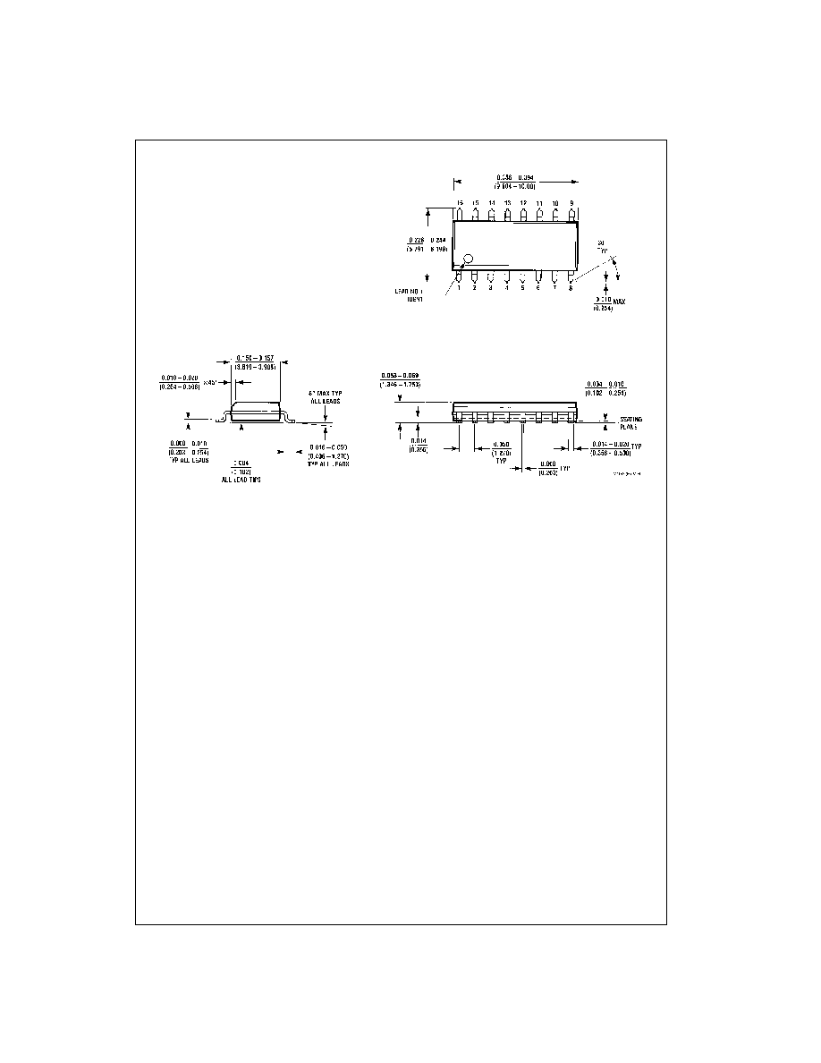
Physical Dimensions
inches (millimeters) unless otherwise noted
16-Lead Small Outline Integrated Circuit (SOIC), JEDEC MS-012, 0.150 Narrow
Package Number M16A

www.fairchildsemi.com
8
D
M
96LS02
Dual
Ret
r
i
ggerabl
e
Resett
abl
e Monost
able
Mult
iv
ibr
a
tor
Physical Dimensions
inches (millimeters) unless otherwise noted (Continued)
16-Lead Plastic Dual-In-Line Package (PDIP), JEDEC MS-001, 0.300 Wide
Package Number N16E
Fairchild does not assume any responsibility for use of any circuitry described, no circuit patent licenses are implied and
Fairchild reserves the right at any time without notice to change said circuitry and specifications.
LIFE SUPPORT POLICY
FAIRCHILD'S PRODUCTS ARE NOT AUTHORIZED FOR USE AS CRITICAL COMPONENTS IN LIFE SUPPORT
DEVICES OR SYSTEMS WITHOUT THE EXPRESS WRITTEN APPROVAL OF THE PRESIDENT OF FAIRCHILD
SEMICONDUCTOR CORPORATION. As used herein:
1. Life support devices or systems are devices or systems
which, (a) are intended for surgical implant into the
body, or (b) support or sustain life, and (c) whose failure
to perform when properly used in accordance with
instructions for use provided in the labeling, can be rea-
sonably expected to result in a significant injury to the
user.
2. A critical component in any component of a life support
device or system whose failure to perform can be rea-
sonably expected to cause the failure of the life support
device or system, or to affect its safety or effectiveness.
www.fairchildsemi.com