 | ÐлекÑÑоннÑй компоненÑ: ACE12022B | СкаÑаÑÑ:  PDF PDF  ZIP ZIP |
Äîêóìåíòàöèÿ è îïèñàíèÿ www.docs.chipfind.ru
1
www.fairchildsemi.com
ACE1202 Product Family Rev. B.1
ACE1202 Product Family Arithmetic Controller Engine (ACExTM) for Low Power Applications
ACE1202 Product Family
Arithmetic Controller Engine (ACExTM)
for Low Power Applications
General Description
The ACE1202 (Arithmetic Controller Engine) family of
microcontrollers is a dedicated programmable monolithic inte-
grated circuit for applications requiring high performance, low
power, and small size. It is a fully static part fabricated using
CMOS technology.
The ACE1202 product family has an 8-bit microcontroller core, 64
bytes of RAM, 64 bytes of data EEPROM and 2K bytes of code
EEPROM. Its on-chip peripherals include a multi-function 16-bit
timer, watchdog/idle timer, and programmable undervoltage de-
tection circuitry. The on-chip clock and reset functions reduce the
number of required external components. The ACE1202 product
family is available in 8- and 14-pin SOIC and DIP packages.
Features
I Arithmetic Controller Engine
I 2K bytes on-board code EEPROM
I 64 bytes data EEPROM
I 64 bytes RAM
I Instruction set geared for block encryption
I Watchdog
I Multi-input wake-up on all I/O pins
I 16-bit multifunction timer with difference capture
I 12-bit idle timer
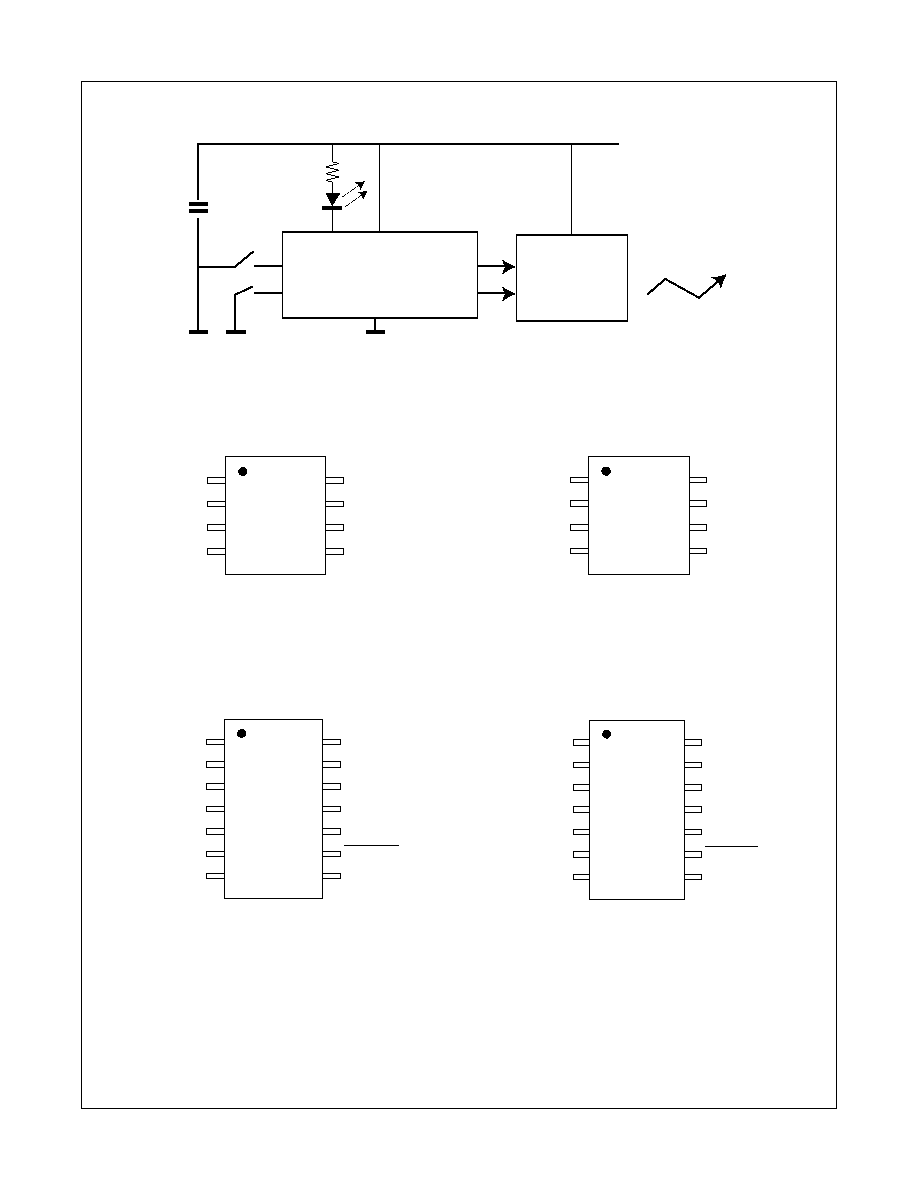
Block and Connection Diagram
PRELIMINARY
August 2001
I Hardware Bit - Coder (HBC) (ACE1202-2 only)
I On-chip oscillator
-- No external components
-- 1
µs instruction cycle time
I On-chip Power-on Reset
I Programmable read and write disable functions
I Memory mapped I/O
I Multilevel Low Voltage Detection
I Brown-out Reset
I Software selectable I/O option
-- Push-pull outputs with tri-state option
-- Weak pull-up or high impedance
I Fully static CMOS
-- Low power HALT mode (100nA @ 3.3V)
-- Power saving IDLE mode
I Single supply operation
-- 1.8-5.5V (P.N. ACE1202L)
-- 2.2-5.5V (P.N. ACE1202, ACE12022)
-- 2.7-5.5V (P.N. ACE1202B, ACE12022B)
I 40 years data retention
I 1,000,000 data changes
I 8 and 14-pin SOIC, 8 and 14-pin DIP packages. (CSP
package available upon request)
I In-circuit programming
VCC
1
Power-on Reset
Brown-out Reset/Low
Battery Detect
ACE1202 core
(4 interrupt
sources
and vectors)
Programming Interface
2K bytes of Code
EEPROM
64 bytes of Data
EEPROM
64 bytes of RAM
12-bit Timer0 with
Watchdog Timer
16-bit Multi-function
Timer1 with Difference
Capture
HALT & IDLE Power
Saving Modes
GPORT
general
purpose
I/O with
multi-
input
wakeup
Internal Oscillator
GND
1
RESET
2
(CKO) G0
(CKI) G1
(T1/TX
3
) G2
G4
(TX
3
) G5
G6
2
G7
2
(Input only) G3
Hardware Bit-Coder
3
© 2001 Fairchild Semiconductor Corporation
1. 100nf Decoupling capacitor recommended
2. Available only in the 14-pin package option
3. Available only on the ACE1202-2 device
2
www.fairchildsemi.com
ACE1202 Product Family Rev. B.1
ACE1202 Product Family Arithmetic Controller Engine (ACExTM) for Low Power Applications
VCC
VCC
Optional
LED
RF Stage
RF Interface
G0
G1
G5
G2
GND
G4
G3
Figure 2: ACEx Application Example (Remote Keyless Entry)
LOAD
VCC
GND
SFT_OUT
CKI
1
2
3
4
5
6
7
8
SFT_IN
NC/VCC
NC
G3
VCC
GND
G1
1
2
3
4
5
6
7
8
G4
NC
9
10
11
12
13
14
G6
G7
G5
NC
NC
G2
RESET
G0
G3
VCC
GND
G2
G1
1
2
3
4
5
6
7
8
G4
G0
G5
LOAD
VCC
GND
CKI
1
2
3
4
5
6
7
8
SFT_IN
NC
NC
9
10
11
12
13
14
NC
NC
NC/VCC
NC
NC
SFT_OUT
RESET
Figure 3: ACE1202/ACE1202-2 8-pin Device Pinout
b) Programming Mode Operation
Figure 4: ACE1202/ACE1202-2 14-pin Device Pinout
b) Programming Mode Operation
a) Normal Mode Operation
a) Normal Mode Operation
3
www.fairchildsemi.com
ACE1202 Product Family Rev. B.1
ACE1202 Product Family Arithmetic Controller Engine (ACExTM) for Low Power Applications
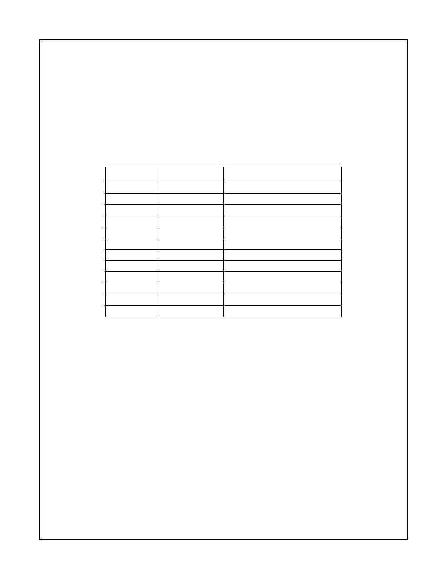
Absolute Maximum Ratings
Ambient Storage Temperature
-65
°C to +150°C
Input Voltage not including G3
-0.3V to V
CC
+0.3V
G3 Input Voltage
0.3V to 13V
Lead Temperature (10s max)
+300
°C
Electrostatic Discharge on all pins
2000V min
Operating Conditions
Relative Humidity (non-condensing)
95%
EEPROM write limits
See DC Electrical
Characteristics
2.0 Electrical Characteristics
Part Number Operating Voltage Ambient Operating Temperature
ACE1202
2.2 to 5.5V
0
°C to 70°C
ACE12022
2.2 to 5.5V
0
°C to 70°C
ACE1202E
2.2 to 5.5V
-40
°C to +85°C
ACE12022E
2.2 to 5.5V
-40
°C to +85°C
ACE1202V
2.2 to 5.5V
-40
°C to +125°C
ACE1202B
2.7 to 5.5V
0
°C to 70°C
ACE12022B
2.7 to 5.5V
0
°C to 70°C
ACE1202BE
2.7 to 5.5V
-40
°C to +85°C
ACE12022BE
2.7 to 5.5V
-40
°C to +85°C
ACE1202BV
2.7 to 5.5V
-40
°C to +125°C
ACE12022BV
2.7 to 5.5V
-40
°C to +125°C
ACE1202L
1.8 to 5.5V
0
°C to 70°C
4
www.fairchildsemi.com
ACE1202 Product Family Rev. B.1
ACE1202 Product Family Arithmetic Controller Engine (ACExTM) for Low Power Applications
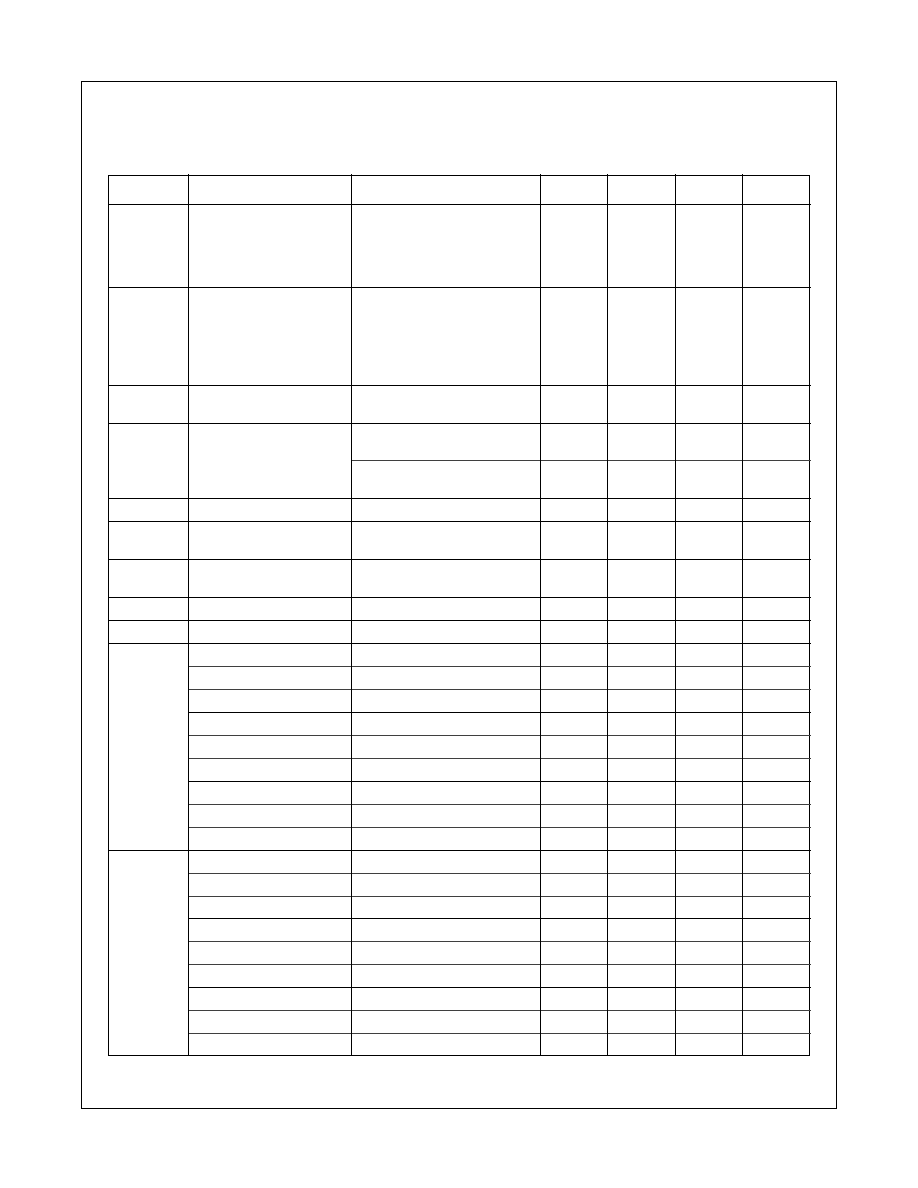
Preliminary ACE1202/ACE1202-2 DC Electrical Characteristics
V
CC
= 1.8/2.2/2.7 to 5.5V
All measurements valid for ambient operating temperature range unless otherwise stated.
Symbol
Parameter
Conditions
MIN
TYP
MAX
Units
I
CC
4
Supply Current
1.8V
0.2
0.5
mA
no data EEPROM write in
2.2V
0.4
1.0
mA
progress
2.7V
0.7
1.2
mA
3.3V
1.2
2.0
mA
5.5V
3.7
5.5
mA
I
CCH
HALT Mode current
3.3V @ -40
°C to +25°C
10
100
nA
5.5V @ -40
°C to +25°C
60
1000
nA
3.3V @ +85
°C
75
1000
nA
5.5V @ +85
°C
400
2500
nA
3.3V @ +125
°C
600
5000
nA
5.5V @+125
°C
1550
8000
nA
I
CCL
5
IDLE Mode Current
3.3V
150
200
µA
5.5V
200
300
µA
V
CCW
EEPROM Write Voltage
Code EEPROM in
4.5
5.0
5.5
V
Programming Mode
Data EEPROM in
2.4
5.5
V
Operating Mode
S
VCC
Power Supply Slope
1
µs/V
10ms/V
V
IL
Input Low with Schmitt
V
CC
= 1.8 -5.5V
0.2V
CC
V
Trigger Buffer
V
IH
Input High with Schmitt
V
CC
= 1.8 - 5.5V
0.8V
CC
V
Trigger Buffer
I
IP
Input Pull-up Current
V
CC
=5.5V, V
IN
=0V
30
65
350
µA
I
TL
TRI-STATE Leakage
V
CC
=5.5V
2
200
nA
V
OL
Output Low Voltage
V
CC
= 1.8 - 2.2V
G0, G1, G2, G4, G6, G7
0.8 mA sink
0.2V
CC
V
G5
1.0 mA sink
0.2V
CC
V
Output Low Voltage
V
CC
= 2.2V 3.3V
G0, G1, G2, G4, G6, G7
3.0 mA sink
0.2V
CC
V
G5
5.0 mA sink
0.2V
CC
V
Output Low Voltage
V
CC
= 3.3V 5.5V
G0, G1, G2, G4, G6, G7
5.0 mA sink
0.2V
CC
V
G5
10.0 mA sink
0.2V
CC
V
V
OH
Output High Voltage
V
CC
= 1.8 - 2.2V
G0, G1, G2, G4, G6, G7
0.1 mA source
0.8V
CC
V
G5
0.2 mA source
0.8V
CC
V
Output High Voltage
V
CC
= 3.3V 5.5V
G0, G1, G2, G4, G6, G7
0.4 mA source
0.8V
CC
V
G5
0.8 mA source
0.8V
CC
V
Output High Voltage
V
CC
= 3.3V 5.5V
G0, G1, G2, G4, G6, G7
0.4 mA source
0.8V
CC
V
G5
1.0 mA source
0.8V
CC
V
4
I
CC
active current is dependent on the program code.
5
Based on a continuous IDLE looping program.
5
www.fairchildsemi.com
ACE1202 Product Family Rev. B.1
ACE1202 Product Family Arithmetic Controller Engine (ACExTM) for Low Power Applications
Preliminary ACE1202/ACE1202-2 AC Electrical Characteristics
V
CC
= 1.8/2.2/2.7 to 5.5V
All measurements valid for ambient operating temperature range unless otherwise stated.
Parameter
Conditions
MIN
TYP
MAX
Units
Instruction cycle time from
5.0V at +25
°C
0.9
1.0
1.1
µs
internal clock - setpoint
Internal clock voltage dependent
3.0V to 5.5V,
+5
%
frequency variation
constant temperature
Internal clock temperature
3.0V to 5.5V,
+10
%
dependent frequency variation
full temperature range
Internal clock frequency
3.0V to 4.5V,
+2
%
deviation for 0.5V drop
constant temperature
Crystal oscillator frequency
(Note 6)
4
MHz
External clock frequency
(Note 7)
4
MHz
EEPROM write time
3
10
ms
Internal clock start up time
(Note 7)
2
ms
Oscillator start up time
(Note 7)
2400
cycles
6
The maximum permissible frequency is guaranteed by design but not 100% tested.
7
The parameter is guaranteed by design but not 100% tested.
Preliminary ACE1202/ACE1202-2 Electrical Characteristics for programming
All data following is valid between 4.5V and 5.5V at ambient temperature. The following charac-
teristics are guaranteed by design but are not 100% tested. See "EEPROM write time" in the AC
Electrical Characteristics for definition of the programming ready time.
Parameter
Description
MIN
MAX
Units
t
HI
CLOCK high time
500
DC
ns
t
LO
CLOCK low time
500
DC
ns
t
DIS
SHIFT_IN setup time
100
ns
t
DIH
SHIFT_IN hold time
100
ns
t
DOS
SHIFT_OUT setup time
100
ns
t
DOH
SHIFT_OUT hold time
900
ns
t
SV1
, t
SV2
LOAD supervoltage timing
50
µs
t
LOAD1
, t
LOAD2
, t
LOAD3
, t
LOAD4
LOAD timing
5
µs
V
SUPERVOLTAGE
Supervoltage level
11.5
12.5
V